2SK1530O 查看數據表(PDF) - Toshiba
零件编号
产品描述 (功能)
生产厂家
2SK1530O Datasheet PDF : 4 Pages
| |||
TOSHIBA Field Effect Transistor Silicon N Channel MOS Type
2SK1530
2SK1530
High-Power Amplifier Application
z High breakdown voltage
z High forward transfer admittance
z Complementary to 2SJ201
: VDSS = 200 V
: |Yfs| = 5.0 S (typ.)
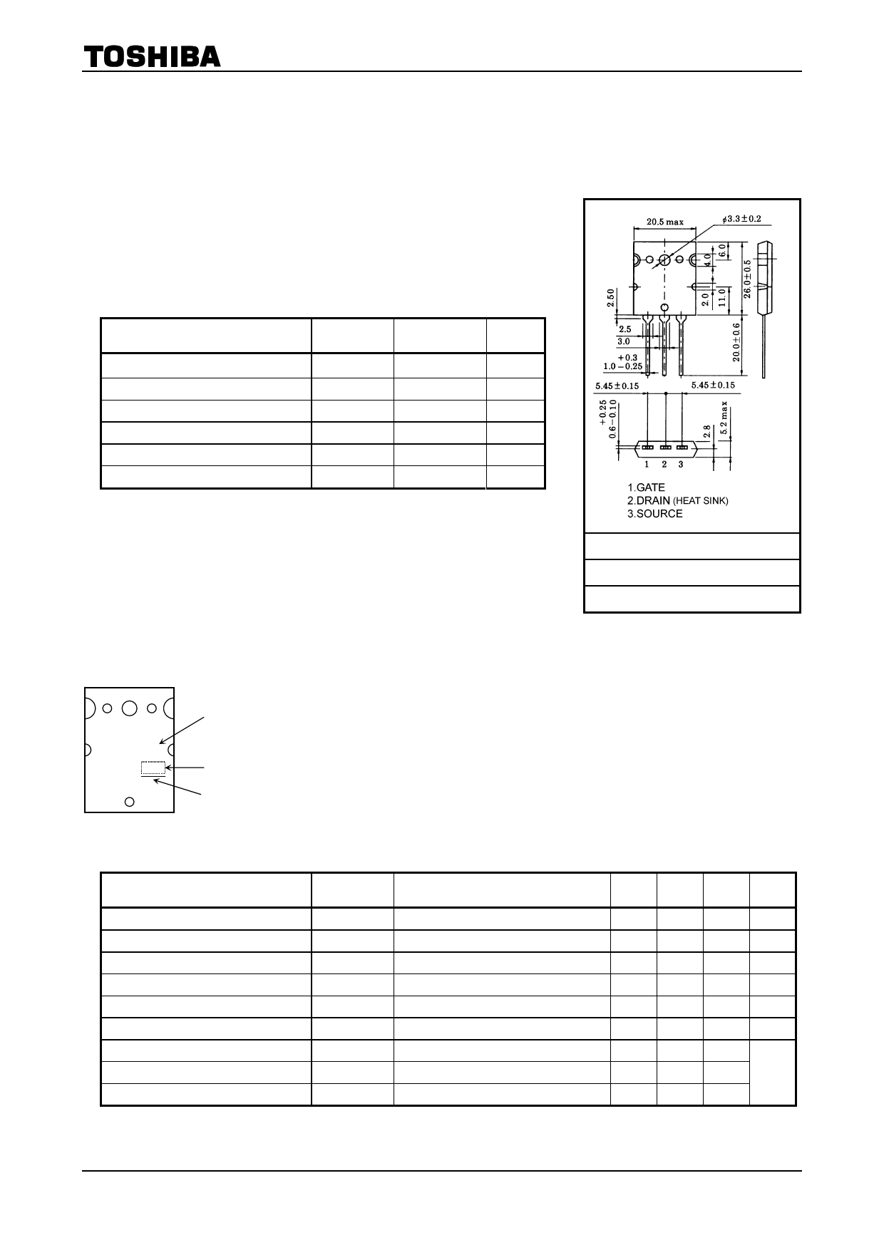
Unit: mm
Absolute Maximum Ratings (Ta = 25°C)
Characteristics
Symbol
Rating
Unit
Drain−source voltage
Gate−source voltage
Drain current
(Note 1)
Drain power dissipation (Tc = 25°C)
Channel temperature
Storage temperature range
VDSS
VGSS
ID
PD
Tch
Tstg
200
V
±20
V
12
A
150
W
150
°C
−55 to 150
°C
Note: Using continuously under heavy loads (e.g. the application of high
temperature/current/voltage and the significant change in temperature, etc.)
may cause this product to decrease in the reliability significantly even if the
operating conditions (i.e. operating temperature/current/voltage, etc.) are
within the absolute maximum ratings. Please design the appropriate reliability
upon reviewing the Toshiba Semiconductor Reliability Handbook (“Handling
Precautions”/“Derating Concept and Methods”) and individual reliability data
(i.e. reliability test report and estimated failure rate, etc).
Note 1: Ensure that the channel temperature does not exceed 150°C.
JEDEC
―
JEITA
―
TOSHIBA
2-21F1B
Weight: 9.75 g (typ.)
Marking
Note 2: A line under a Lot No. identifies the indication of product
TOSHIBA
2SK1530
Part No. (or abbreviation code)
Labels.
Not underlined: [[Pb]]/INCLUDES > MCV
Underlined: [[G]]/RoHS COMPATIBLE or [[G]]/RoHS [[Pb]]
Lot No.
Please contact your TOSHIBA sales representative for details as to
JAPAN
Note 2
environmental matters such as the RoHS compatibility of Product. The
RoHS is the Directive 2002/95/EC of the European Parliament and of
the Council of 27 January 2003 on the restriction of the use of certain
hazardous substances in electrical and electronic equipment.
Electrical Characteristics (Ta = 25°C)
Characteristics
Symbol
Test Condition
Drain cut−off current
Gate leakage current
Drain−source breakdown voltage
Drain−source saturation voltage
Gate−source cut−off voltage (Note 3)
Forward transfer admittance
Input capacitance
Output capacitance
Reverse transfer capacitance
IDSS
IGSS
V (BR) DSS
VDS (ON)
VGS (OFF)
|Yfs|
Ciss
Coss
Crss
VDS = 200 V, VGS = 0
VDS = 0V, VGS = ±20 V
ID = 10 mA, VGS = 0
ID = 8 A, VGS = 10 V
VDS = 10 V, ID = 0.1 A
VDS = 10 V, ID = 5 A
VDS = 30 V, VGS = 0, f = 1 MHz
VDS = 30 V, VGS = 0, f = 1 MHz
VDS = 30 V, VGS = 0, f = 1 MHz
Note 3: VGS (OFF) Classification
0: 0.8 to 1.6 Y: 1.4 to 2.8
This transistor is an electrostatic-sensitive device.
Please handle with caution.
1
Min Typ. Max Unit
—
—
1.0 mA
—
— ±0.5 μA
200
—
—
V
—
2.5 5.0
V
0.8
—
2.8
V
—
5.0
—
S
— 900 —
— 180 —
pF
— 100 —
2009-12-21
Share Link: 