2SK3070 查看數據表(PDF) - Renesas Electronics
零件编号
产品描述 (功能)
生产厂家
2SK3070 Datasheet PDF : 9 Pages
| |||
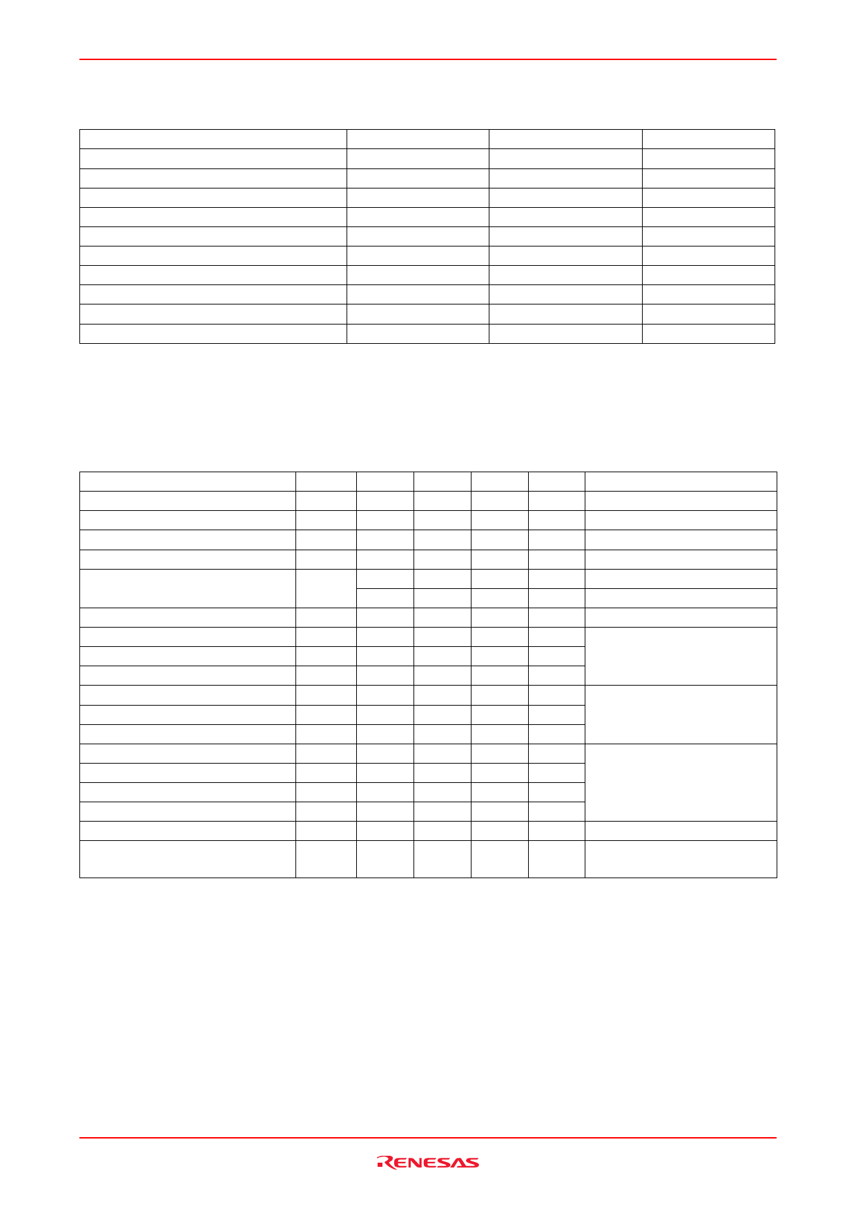
2SK3070(L), 2SK3070(S)
Absolute Maximum Ratings
Item
Drain to source voltage
Gate to source voltage
Drain current
Drain peak current
Body-drain diode reverse drain current
Avalanche current
Avalanche energy
Channel dissipation
Channel temperature
Storage temperature
Notes: 1. PW ≤ 10µs, duty cycle ≤ 1 %
2. Value at Tc = 25°C
3. Value at Tch = 25°C, Rg ≥ 50 Ω
Symbol
VDSS
VGSS
ID
I Note1
D(pulse)
IDR
I Note3
AP
E Note3
AR
Pch Note2
Tch
Tstg
Ratings
40
±20
75
300
75
50
333
100
150
–55 to +150
(Ta = 25°C)
Unit
V
V
A
A
A
A
mJ
W
°C
°C
Electrical Characteristics
Item
Symbol Min
Drain to source breakdown voltage V(BR)DSS 40
Gate to source leak current
IGSS
—
Zero gate voltage drain current
IDSS
—
Gate to source cutoff voltage
VGS(off)
1.0
Static drain to source on state
resistance
RDS(on)
—
—
Forward transfer admittance
|yfs|
50
Input capacitance
Ciss
—
Output capacitance
Coss
—
Reverse transfer capacitance
Crss
—
Total gate charge
Qg
—
Gate to source charge
Qgs
—
Gate to drain charge
Qgd
—
Turn-on delay time
td(on)
—
Rise time
tr
—
Turn-off delay time
td(off)
—
Fall time
tf
—
Body–drain diode forward voltage
VDF
—
Body–drain diode reverse recovery
trr
—
time
Note: 4. Pulse test
Typ
—
—
—
—
4.5
6.5
80
6800
1300
380
130
25
30
60
300
550
400
1.05
90
Max
—
±0.1
10
2.5
5.8
10
—
—
—
—
—
—
—
—
—
—
—
—
—
Unit
V
µA
µA
V
mΩ
mΩ
S
pF
pF
pF
nC
nC
nC
ns
ns
ns
ns
V
ns
(Ta = 25°C)
Test Conditions
ID = 10 mA, VGS = 0
VGS = ±20 V, VDS = 0
VDS = 40 V, VGS = 0
ID = 1 mA, VDS = 10 V Note4
ID = 40 A, VGS = 10 V Note4
ID = 40 A, VGS = 4 V Note4
ID = 40 A, VDS = 10 V Note4
VDS = 10 V, VGS = 0,
f = 1 MHz
VDD = 25 V, VGS = 10 V,
ID = 75 A
VGS = 10 V, ID = 40 A,
RL = 0.75 Ω
IF = 75 A, VGS = 0
IF = 75 A, VGS = 0
diF/ dt = 50 A/ µs
Rev.9.00 Sep 07, 2005 page 2 of 8
Share Link: 