2SK3825 查看數據表(PDF) - SANYO -> Panasonic
零件编号
产品描述 (功能)
生产厂家
2SK3825 Datasheet PDF : 4 Pages
| |||
Continued from preceding page.
Parameter
Input Capacitance
Output Capacitance
Reverse Transfer Capacitance
Turn-ON Delay Time
Rise Time
Turn-OFF Delay Time
Fall Time
Total Gate Charge
Gate-to-Source Charge
Gate-to-Drain “Miller” Charge
Diode Forward Voltage
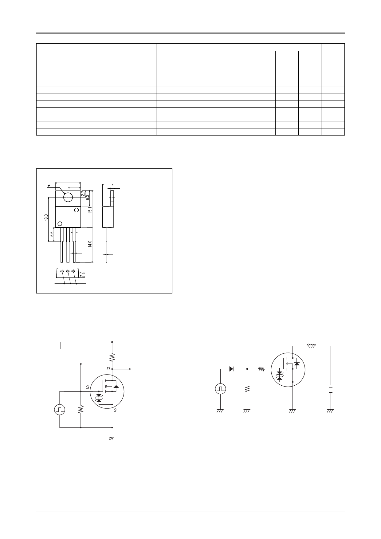
Package Dimensions
unit : mm
2052C
2SK3825
Symbol
Ciss
Coss
Crss
td(on)
tr
td(off)
tf
Qg
Qgs
Qgd
VSD
Conditions
VDS=20V, f=1MHz
VDS=20V, f=1MHz
VDS=20V, f=1MHz
See specified Test Circuit.
See specified Test Circuit.
See specified Test Circuit.
See specified Test Circuit.
VDS=30V, VGS=10V, ID=74A
VDS=30V, VGS=10V, ID=74A
VDS=30V, VGS=10V, ID=74A
IS=74A, VGS=0
10.2
3.6
5.1
4.5
1.3
Ratings
Unit
min
typ
max
5250
pF
780
pF
525
pF
40
ns
315
ns
370
ns
310
ns
113
nC
19
nC
28
nC
1.13
1.5
V
1.2
0.8
123
2.55
2.55
0.4 1 : Gate
2 : Drain
3 : Source
SANYO : TO-220
Switching Time Test Circuit
VIN
10V
0V
VIN
PW=10µs
D.C.≤1%
G
VDD=30V
ID=37A
RL=0.81Ω
D
VOUT
2SK3825
P.G
50Ω
S
Avalanche Resistance Test Circuit
≥50Ω
10V
0V
50Ω
L
2SK3825
VDD
No.8242-2/4
Share Link: 