DSP56F801E 查看數據表(PDF) - Motorola => Freescale
零件编号
产品描述 (功能)
生产厂家
DSP56F801E Datasheet PDF : 44 Pages
| |||
Freescale Semiconductor, Inc.
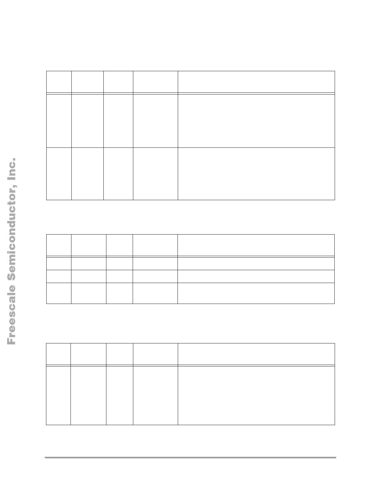
2.7 Serial Communications Interface (SCI) Signals
Table 10. Serial Communications Interface (SCI0) Signals
No. of
Pins
Signal
Name
Signal
Type
State During
Reset
Signal Description
1
TXD0
Output
GPIOB0
Input/
Output
1
RXD0
Input
Input
Input
Input
Transmit Data (TXD0)—SCI0 transmit data output
Port B GPIO—This pin is a General Purpose I/O (GPIO) pin
that can be individually programmed as an input or output
pin.
After reset, the default state is SCI output.
Receive Data (RXD0)—SCI0 receive data input
GPIOB1
Input/
Output
Input
Port B GPIO—This pin is a General Purpose I/O (GPIO) pin
that can be individually programmed as an input or output
pin.
After reset, the default state is SCI input.
2.8 Analog-to-Digital Converter (ADC) Signals
Table 11. Analog to Digital Converter Signals
No. of
Pins
Signal
Name
Signal State During
Type
Reset
Signal Description
4
ANA0-3
Input
4
ANA4-7
Input
1
VREF
Input
Input
Input
Input
ANA0-3—Analog inputs to ADC, channel 1
ANA4-7—Analog inputs to ADC, channel 2
VREF—Analog reference voltage for ADC. Must be set to
VDDA-0.3V for optimal performance.
2.9 Quad Timer Module Signals
Table 12. Quad Timer Module Signals
No. of
Pins
Signal
Name
Signal State During
Type
Reset
Signal Description
3
TD0-2
Input/
Output
GPIOA0-2 Input/
Output
Input
Input
TD0-2—Timer D Channel 0-2
Port A GPIO—This pin is a General Purpose I/O (GPIO) pin
that can be individually programmed as an input or output
pin.
After reset, the default state is the quad timer input.
10
56F801 Technical Data
For More Information On This Product,
Go to: www.freescale.com
Share Link: 