73S8023C-IM 查看數據表(PDF) - Teridian Semiconductor Corporation
零件编号
产品描述 (功能)
生产厂家
73S8023C-IM Datasheet PDF : 27 Pages
| |||
73S8023C Data Sheet
DS_8023C_019
1.4 Microcontroller Interface
Name
CMDVCC
5V/#V
PWRDN
CLKDIV1
CLKDIV2
Pin Description
18 Command VCC (negative assertion): Logic low on this pin causes the DC-DC
converter to ramp the VCC supply to the card and initiates a card activation
sequence.
31 5 volt / 3 volt card selection: Logic one selects 5 volts for VCC and card
interface, logic low selects 3 volt operation. When the part is to be used with
a single card voltage, this pin should be tied to either GND or VDD. However,
it includes a high impedance pull-up resistor to default this pin high (selection
of 5V card) when unconnected
5
Power Down control input: Active High. When Power Down (PD) mode is
activated, all internal analog functions are disabled to place the 73S8023C in
its lowest power consumption mode. The PD mode is allowed only out of a
card session (PWRDN high is ignored when CMDVCC = 0). Must be tied to
ground when power down function is not used.
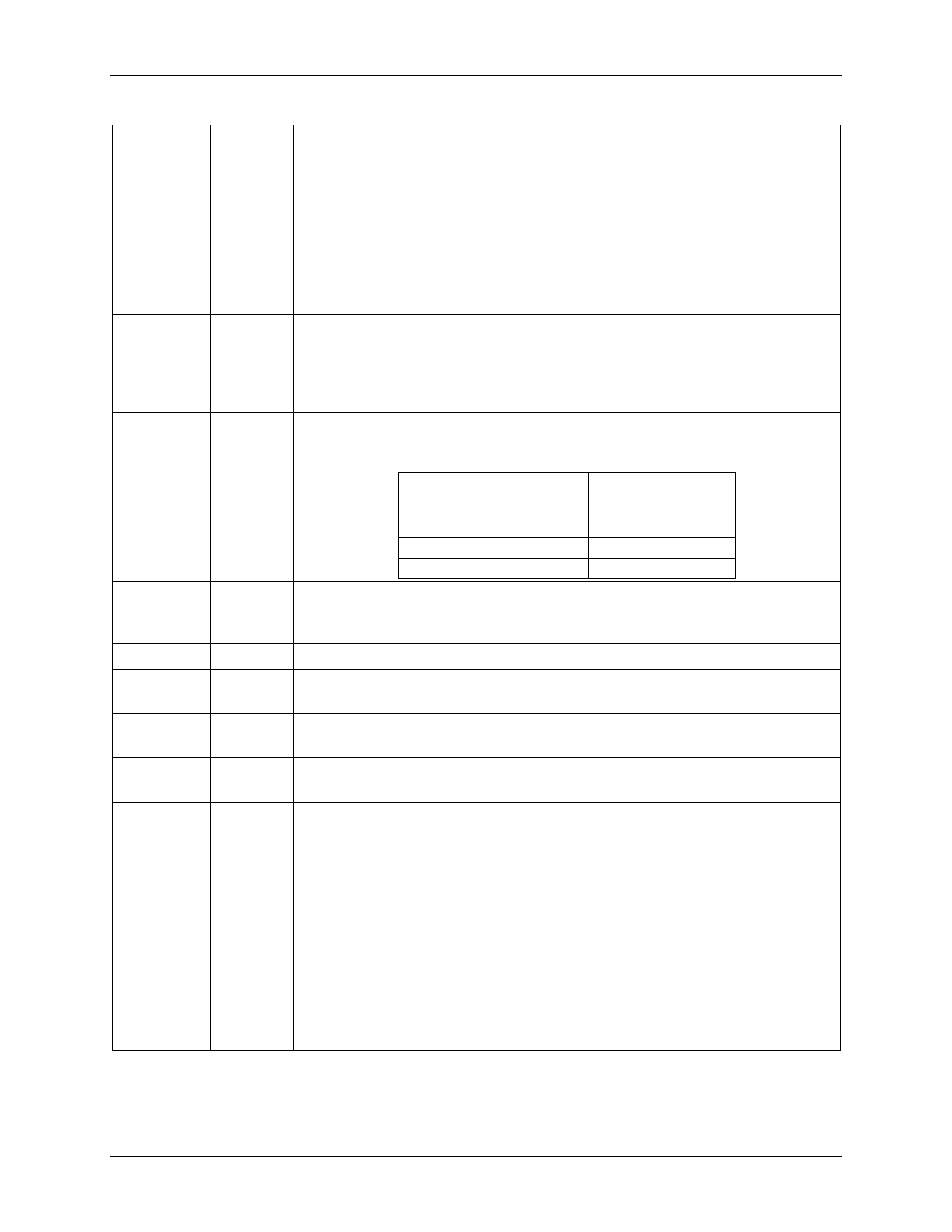
29 Sets the divide ratio from the XTALIN oscillator (or external clock input) to the
30 card clock. These pins include pull-down resistors.
OFF
RSTIN
I/OUC
AUX1UC
AUX2UC
CS
CLKSEL
STROBE
CLKOUT
CLKDIV1 CLKDIV2
Clock Rate
0
0
XTALIN/8
0
1
XTALIN/4
1
1
XTALIN/2
1
0
XTALIN
22 Interrupt signal to the processor: Active Low. Multi-function indicating fault
conditions and card presence. Open drain output configuration; it includes an
internal 20 kΩ pull-up to VDD.
19 Reset Input: This signal controls the RST signal to the card.
26 System controller data I/O to/from the card. Includes internal pull-up resistor
to VDD.
27 System controller auxiliary data I/O to/from the card. Includes internal pull-up
resistor to VDD.
28 System controller auxiliary data I/O to/from the card. Includes internal pull-up
resistor to VDD.
8
When CS = 1, the control and signal pins are configured normally. When CS
is set low, signals CMDVCC, RSTIN, PWRDN, 5V/#V, CLKDIV1, CLKDIV2,
CLKSEL are latched. I/OUC, AUX1UC, and AUX2UC are set to high
impedance pull-up mode and won’t pass data to or from the smart card. OFF
output is tri-stated.
16 Selects CLK and RST operational mode. When CLKSEL is low (default), the
circuit is configured for asynchronous card operation and the sequencer
manages the control of CLK and RST. When CLKSEL is high, the signal
CLK is a buffered copy of STROBE and the signal RST is directly controlled
by RSTIN.
25 When CLKSEL = 1, the signal CLK is controlled directly by STROBE.
32 CLKOUT is the buffered version of the signal on pin XTALIN.
6
Rev. 1.5
Share Link: 