74ABT16260DL(2002) 查看數據表(PDF) - Philips Electronics
零件编号
产品描述 (功能)
生产厂家
74ABT16260DL Datasheet PDF : 12 Pages
| |||
Philips Semiconductors
12-bit to 24-bit multiplexed D-type latch (3-State)
Product data
74ABT16260
FEATURES
• ESD protection exceeds 2000 V per Mil-Std-883C, Method 3015;
exceeds 200 V using machine model (C = 200 pF, R = 0).
• Latch-up performance exceeds 500 mA per JEDEC Standard
JESD-17.
• Distributed VCC and GND pin configuration minimizes high-speed
switching noise.
• Flow-through architecture optimizes PCB layout.
• High-drive outputs (–32 mA IOH, 64 mA IOL).
• Package options:
– 56-pin plastic Shrink Small-Outline Package (SSOP)
– 56-pin plastic Thin Shrink Small-Outline Package (TSSOP)
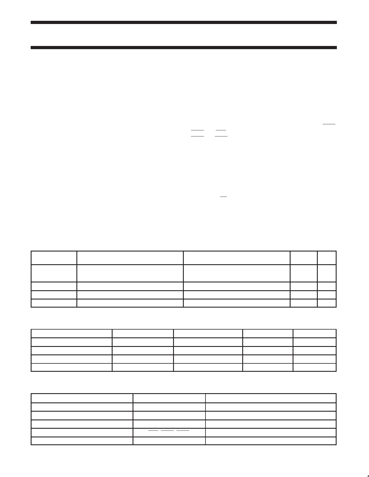
QUICK REFERENCE DATA
SYMBOL
PARAMETER
tPLH
tPHL
CIN
COUT
ICCZ
Propagation delay
nAx to nBx nBx to nAx
Input capacitance
Output capacitance
Total supply current
DESCRIPTION
The 74ABT16260 is a 12-bit to 24-bit multiplexed D-type latch used
in applications where two separate data paths must be multiplexed
onto, or demultiplexed from, a single data path. Typical applications
include multiplexing and/or demultiplexing of address and data
information in microprocessor or bus-interface applications. This
device is also useful in memory-interleaving applications.
Three 12-bit I/O ports (A1–A12, 1B1–1B12, and 2B1–2B12) are
available for address and/or data transfer. The output enable (OE1B,
OE2B, and OEA) inputs control the bus transceiver functions. The
OE1B and OE2B control signals also allow bank control in the
A-to-B direction.
Address and/or data information can be stored using the internal
storage latches. The latch enable (LE1B, LE2B, LEA1B, and
LEA2B) inputs are used to control data storage. When the latch
enable input is HIGH, the latch is transparent. When the latch
enable input goes LOW, the data present at the inputs is latched and
remains latched until the latch enable input is returned HIGH.
To ensure the high-impedance state during power-up or
power-down, OE should be tied to VCC through a pull-up resistor;
the minimum value of the resistor is determined by the current
sinking capability of the driver.
CONDITIONS
Tamb = 25°C; GND = 0V
CL = 50 pF
VI = 0 V or VCC
VI/O = 0 V or 5.0 V
Outputs disabled
TYPICAL UNIT
2.8
ns
2.5
4
pF
6
pF
100
µA
ORDERING INFORMATION
PACKAGES
56-Pin Plastic SSOP Type III
56-Pin Plastic TSSOP Type II
TEMPERATURE RANGE
–40 °C to +85 °C
–40 °C to +85 °C
ORDER CODE
74ABT16260DL
74ABT16260DGG
DWG NUMBER
SOT371-1
SOT364-1
PIN DESCRIPTION
PIN NUMBER
8, 9, 10, 12, 13, 14, 15, 16, 17, 19, 20, 21
23, 24, 26, 31, 33, 34, 36, 37, 38, 40, 41, 42
6, 5, 3, 54, 52, 51, 49, 48, 47, 45, 44, 43
1, 29, 56
2, 27, 30, 55
SYMBOL
An
1Bn
2Bn
OEA, OE1B, OE2B
LE1B, LE2B, LEA1B, LEA2B
FUNCTION
Data inputs/outputs (A)
Data inputs/outputs (B1)
Data inputs/outputs (B2)
Output enable input (Active-LOW)
Latch enable inputs
2002 Apr 03
2
853-2048 27958
Share Link: 