74F113 查看數據表(PDF) - Philips Electronics
零件编号
产品描述 (功能)
生产厂家
74F113 Datasheet PDF : 10 Pages
| |||
Philips Semiconductors
Dual J-K negative edge-triggered flip-flops
without reset
Product specification
74F113
FEATURE
• Industrial temperature range available (–40°C to +85°C)
DESCRIPTION
The 74F113, dual negative edge-triggered JK-type flip-flop, features
individual J, K, clock (CP), set (SD) inputs, true and complementary
outputs. The asynchronous SD input, when low, forces the outputs
to the steady state levels as shown in the function table regardless
of the level at the other inputs.
A high level on the clock (CP) input enables the J and K inputs and
data will be accepted. The logic levels at the J and K inputs may be
allowed to change while the CP is high and flip-flop will perform
according to the function table as long as minimum setup and hold
times are observed. Output changes are initiated by the high-to-low
transition of the CP.
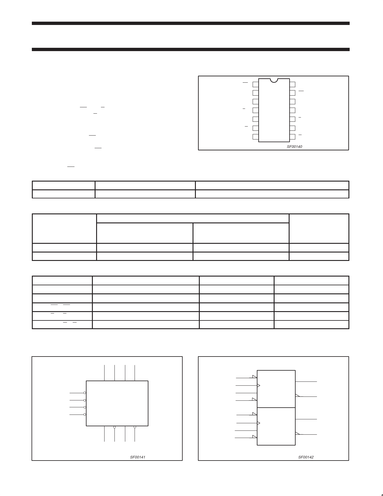
PIN CONFIGURATION
CP0 1
K0 2
J0 3
SD0 4
Q0 5
Q0 6
GND 7
14 VCC
13 CP1
12 K1
11 J1
10 SD1
9 Q1
8 Q1
SF00140
TYPE
74F113
TYPICAL fmax
100MHz
TYPICAL SUPPLY CURRENT (TOTAL)
15mA
ORDERING INFORMATION
ORDER CODE
DESCRIPTION
14-pin plastic DIP
COMMERCIAL RANGE
VCC = 5V ±10%,
Tamb = 0°C to +70°C
N74F113N
INDUSTRIAL RANGE
VCC = 5V ±10%,
Tamb = –40°C to +85°C
I74F113N
14-pin plastic SO
N74F113D
I74F113D
PKG. DWG. #
SOT27–1
SOT108–1
INPUT AND OUTPUT LOADING AND FAN-OUT TABLE
PINS
DESCRIPTION
74F (U.L.) HIGH/LOW
J0, J1
J inputs
1.0/1.0
K0, K1
K inputs
1.0/1.0
CP0, CP1
Clock inputs (active falling edge)
1.0/4.0
SD0, SD1
Set inputs (active low)
1.0/5.0
Q0, Q1, Q0, Q1
Data outputs
50/33
NOTE:
One (1.0) FAST unit load is defined as: 20µA in the High state and 0.6mA in the Low state.
LOAD VALUE HIGH/LOW
20µA/0.6mA
20µA/0.6mA
20µA/2.4mA
20µA/3.0mA
1.0mA/20mA
LOGIC SYMBOL
3 11 2 12
IEC/IEEE SYMBOL
1
4
13
10
VCC = Pin 14
GND = Pin 7
J0 J1 K0 K1
CP0
SD0
CP1
SD1
Q0 Q0 Q1 Q1
56 98
SF00141
3
1J
1
C1
2
1K
4
1S
11
2J
13
C2
12
2K
10
2S
5
6
9
8
SF00142
1996 Mar 14
2
853–0339 16575
Share Link: 