DM74LS367ANX 查看數據表(PDF) - Fairchild Semiconductor
零件编号
产品描述 (功能)
生产厂家
DM74LS367ANX Datasheet PDF : 4 Pages
| |||
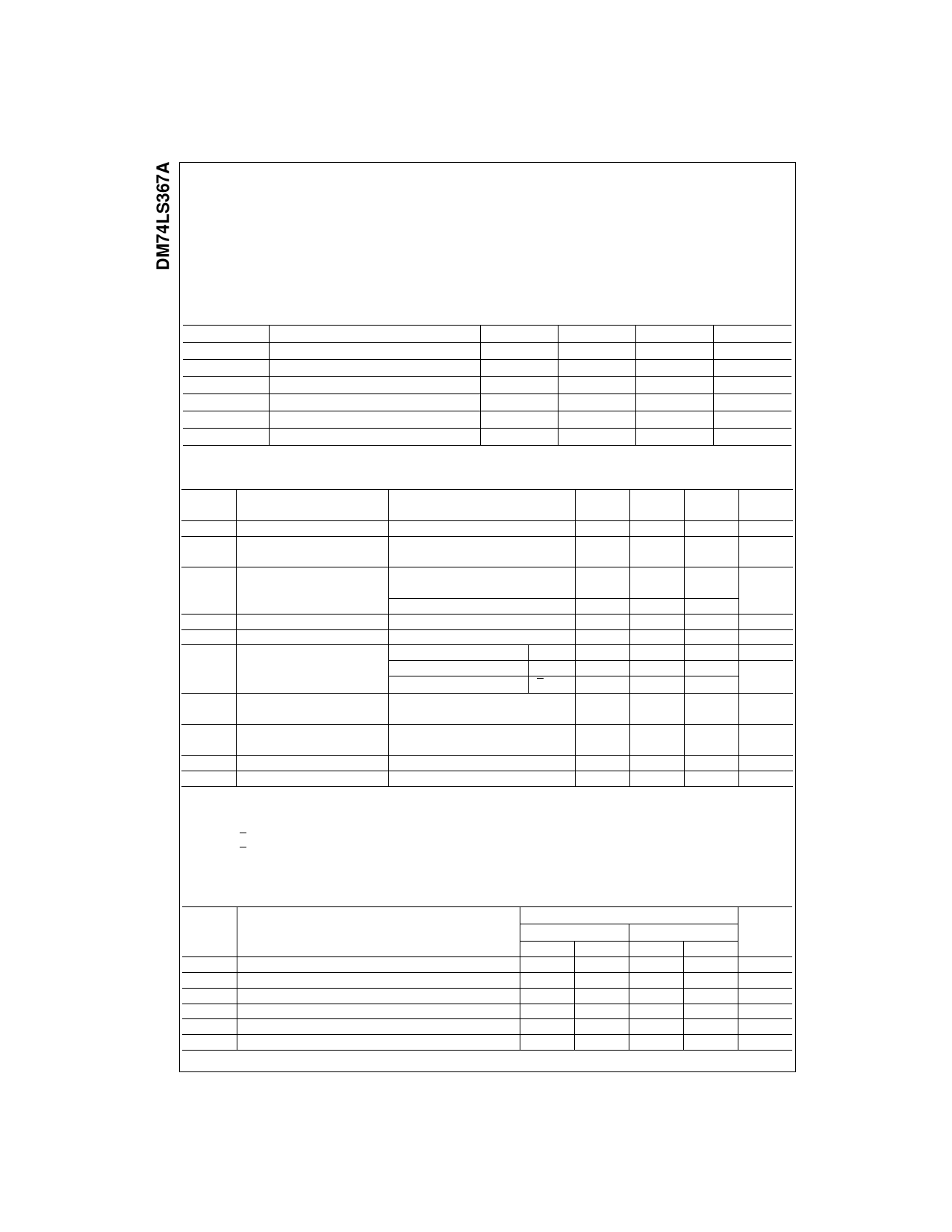
Absolute Maximum Ratings(Note 1)
Supply Voltage
7V
Input Voltage
7V
Operating Free Air Temperature Range 0°C to +70°C
Storage Temperature Range
−65°C to +150°C
Note 1: The “Absolute Maximum Ratings” are those values beyond which
the safety of the device cannot be guaranteed. The device should not be
operated at these limits. The parametric values defined in the Electrical
Characteristics tables are not guaranteed at the absolute maximum ratings.
The “Recommended Operating Conditions” table will define the conditions
for actual device operation.
Recommended Operating Conditions
Symbol
VCC
VIH
VIL
IOH
IOL
TA
Parameter
Supply Voltage
HIGH Level Input Voltage
LOW Level Input Voltage
HIGH Level Output Current
LOW Level Output Current
Free Air Operating Temperature
Min
4.75
2
0
Nom
5
Max
5.25
0.8
−2.6
24
70
Units
V
V
V
mA
mA
°C
Electrical Characteristics
over recommended operating free air temperature range (unless otherwise noted)
Symbol
Parameter
Conditions
Min
VI
Input Clamp Voltage
VCC = Min, II = −18 mA
VOH
HIGH Level
VCC = Min, IOH = Max
2.4
Output Voltage
VIL = Max, VIH = Min
VOL
LOW Level
VCC = Min, IOL = Max
Output Voltage
VIL = Max, VIH = Min
IOL = 12 mA, VCC = Min
II
Input Current @ Max Input Voltage VCC = Max, VI = 7V
IIH
HIGH Level Input Current
VCC = Max, VI = 2.7V
IIL
LOW Level
VCC = Max, VI = 0.5V (Note 5) A Input
Input Current
VCC = Max, VI = 0.4V (Note 6) A Input
IOZH
IOZL
IOS
ICC
VCC = Max, VI = 0.4V
Off-State Output Current with
VCC = Max, VO = 2.4V
HIGH Level Output Voltage Applied VIH = Min, VIL = Max
Off-State Output Current with
VCC = Max, VO = 0.4V
LOW Level Output Voltage Applied VIH = Min, VIL = Max
Short Circuit Output Current
VCC = Max (Note 3)
Supply Current
VCC = Max (Note 4)
G Input
−20
Note 2: All typicals are at VCC = 5V, TA = 25°C.
Note 3: Not more than one output should be shorted at a time, and the duration should not exceed one second.
Note 4: ICC is measured with the DATA inputs grounded and the OUTPUT CONTROLS at 4.5V.
Note 5: Both G inputs are at 2V.
Note 6: Both G inputs at 0.4V.
Typ
(Note 2)
3.4
0.35
0.25
14
Max
−1.5
0.5
0.4
0.1
20
−20
−0.4
−0.4
20
−20
−100
24
Units
V
V
V
mA
µA
µA
mA
µA
µA
mA
mA
Switching Characteristics
at VCC = 5V and TA = 25°C
Symbol
Parameter
tPLH
Propagation Delay Time LOW-to-HIGH Level Output
tPHL
Propagation Delay Time HIGH-to-LOW Level Output
tPZH
Output Enable Time to HIGH Level Output
tPZL
Output Enable Time to LOW Level Output
tPHZ
Output Disable Time from HIGH Level Output (Note 7)
tPLZ
Output Disable Time from LOW Level Output (Note 7)
Note 7: CL = 5 pF.
RL = 667Ω
CL = 50 pF
CL = 150 pF
Min
Max
Min
Max
16
25
16
25
30
40
30
40
20
20
Units
ns
ns
ns
ns
ns
ns
www.fairchildsemi.com
2
Share Link: 