74LVC1G06(2007) 查看數據表(PDF) - NXP Semiconductors.
零件编号
产品描述 (功能)
生产厂家
74LVC1G06 Datasheet PDF : 14 Pages
| |||
NXP Semiconductors
74LVC1G06
Inverter with open-drain output
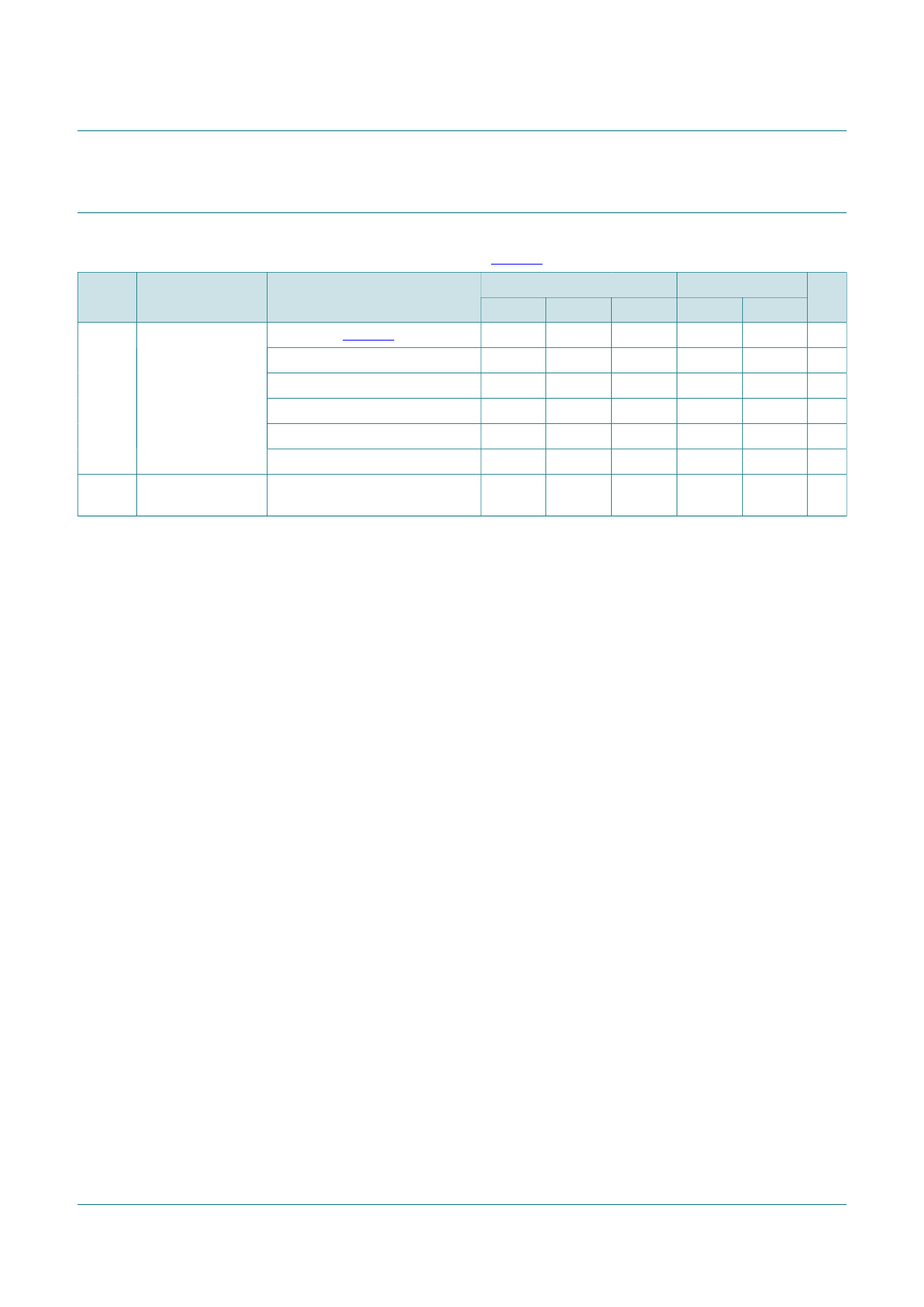
11. Dynamic characteristics
Table 8. Dynamic characteristics
Voltages are referenced to GND (ground = 0 V); for load circuit see Figure 8.
Symbol Parameter
Conditions
−40 °C to +85 °C
Min Typ[1] Max
tpd
propagation delay A to Y; see Figure 7
[2]
VCC = 1.65 V to 1.95 V
1.0
3
6.5
VCC = 2.3 V to 2.7 V
0.5
1.9
4
VCC = 2.7 V
0.5
2.5
4.5
VCC = 3.0 V to 3.6 V
0.5
2.3
4
VCC = 4.5 V to 5.5 V
0.5
1.7
3
CPD
power dissipation VI = GND to VCC; VCC = 3.3 V [3] -
14
-
capacitance
−40 °C to +125 °C Unit
Min
Max
1.0
8.5 ns
0.5
5.5 ns
0.5
6 ns
0.5
5.5 ns
0.5
4 ns
-
- pF
[1] Typical values are measured at Tamb = 25 °C and VCC = 1.8 V, 2.5 V, 2.7 V, 3.3 V and 5.0 V respectively.
[2] tpd is the same as tPLZ and tPZL.
[3] CPD is used to determine the dynamic power dissipation (PD in µW).
PD = CPD × VCC2 × fi × N + ∑(CL × VCC2 × fo) where:
fi = input frequency in MHz;
fo = output frequency in MHz;
CL = output load capacitance in pF;
VCC = supply voltage in V;
N = number of inputs switching;
∑(CL × VCC2 × fo) = sum of outputs.
12. Waveforms
A input
VI
GND
Y output
VCC
VOL
VM
t PLZ
VX
Measurement points are given in Table 9.
VOL is the typical output voltage level that occurs with the output load.
Fig 7. The input A to output Y propagation delay times
t PZL
VM
mna621
74LVC1G06_7
Product data sheet
Rev. 07 — 12 July 2007
© NXP B.V. 2007. All rights reserved.
6 of 14
Share Link: 