74LVC1G06GX(2012) 查看數據表(PDF) - NXP Semiconductors.
零件编号
产品描述 (功能)
生产厂家
74LVC1G06GX Datasheet PDF : 18 Pages
| |||
NXP Semiconductors
74LVC1G06
Inverter with open-drain output
3. Ordering information
Table 1. Ordering information
Type number
Package
Temperature range
74LVC1G06GW
40 C to +125 C
74LVC1G06GV
74LVC1G06GM
40 C to +125 C
40 C to +125 C
74LVC1G06GF
40 C to +125 C
74LVC1G06GN
40 C to +125 C
74LVC1G06GS
40 C to +125 C
74LVC1G06GX
40 C to +125 C
Name
TSSOP5
SC-74A
XSON6
XSON6
XSON6
XSON6
X2SON5
Description
Version
plastic thin shrink small outline package;
5 leads; body width 1.25 mm
SOT353-1
plastic surface-mounted package; 5 leads
SOT753
plastic extremely thin small outline package; SOT886
no leads; 6 terminals; body 1 1.45 0.5 mm
plastic extremely thin small outline package;
no leads; 6 terminals; body 1 1 0.5 mm
SOT891
extremely thin small outline package; no leads; SOT1115
6 terminals; body 0.9 1.0 0.35 mm
extremely thin small outline package; no leads; SOT1202
6 terminals; body 1.0 1.0 0.35 mm
X2SON5: plastic thermal enhanced extremely
thin small outline package; no leads; 5
terminals; body 0.8 0.8 0.35 mm
SOT1226
4. Marking
Table 2. Marking codes
Type number
74LVC1G06GW
74LVC1G06GV
74LVC1G06GM
74LVC1G06GF
74LVC1G06GN
74LVC1G06GS
74LVC1G06GX
Marking[1]
VR
V06
VR
VR
VR
VR
VR
[1] The pin 1 indicator is located on the lower left corner of the device, below the marking code.
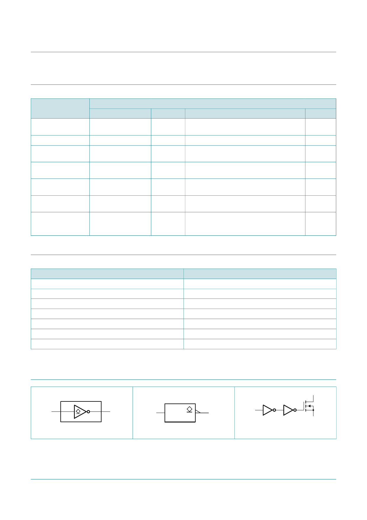
5. Functional diagram
2A
Y4
mna618
Fig 1. Logic symbol
A2
4Y
mna619
Fig 2. IEC logic symbol
Y
A
GND
mna620
Fig 3. Logic diagram
74LVC1G06
Product data sheet
All information provided in this document is subject to legal disclaimers.
Rev. 10 — 29 June 2012
© NXP B.V. 2012. All rights reserved.
2 of 18
Share Link: 