74LVC1G06 查看數據表(PDF) - NXP Semiconductors.
零件编号
产品描述 (功能)
生产厂家
74LVC1G06 Datasheet PDF : 19 Pages
| |||
Nexperia
74LVC1G06
Inverter with open-drain output
3 Ordering information
Table 1. Ordering information
Type number
Package
Temperature range
74LVC1G06GW
-40 °C to +125 °C
74LVC1G06GV
74LVC1G06GM
-40 °C to +125 °C
-40 °C to +125 °C
74LVC1G06GF
-40 °C to +125 °C
74LVC1G06GN
-40 °C to +125 °C
74LVC1G06GS
-40 °C to +125 °C
74LVC1G06GX
-40 °C to +125 °C
Name
TSSOP5
SC-74A
XSON6
XSON6
XSON6
XSON6
X2SON5
Description
Version
plastic thin shrink small outline package;
5 leads; body width 1.25 mm
SOT353-1
plastic surface-mounted package; 5 leads
SOT753
plastic extremely thin small outline package; SOT886
no leads; 6 terminals; body 1 × 1.45 × 0.5 mm
plastic extremely thin small outline package;
no leads; 6 terminals; body 1 × 1 × 0.5 mm
SOT891
extremely thin small outline package; no leads; SOT1115
6 terminals; body 0.9 × 1.0 × 0.35 mm
extremely thin small outline package; no leads; SOT1202
6 terminals; body 1.0 × 1.0 × 0.35 mm
plastic thermal enhanced extremely thin small
outline package; no leads; 5 terminals;
body 0.8 × 0.8 × 0.35 mm
SOT1226
4 Marking
Table 2. Marking codes
Type number
74LVC1G06GW
74LVC1G06GV
74LVC1G06GM
74LVC1G06GF
74LVC1G06GN
74LVC1G06GS
74LVC1G06GX
Marking [1]
VR
V06
VR
VR
VR
VR
VR
[1] The pin 1 indicator is located on the lower left corner of the device, below the marking code.
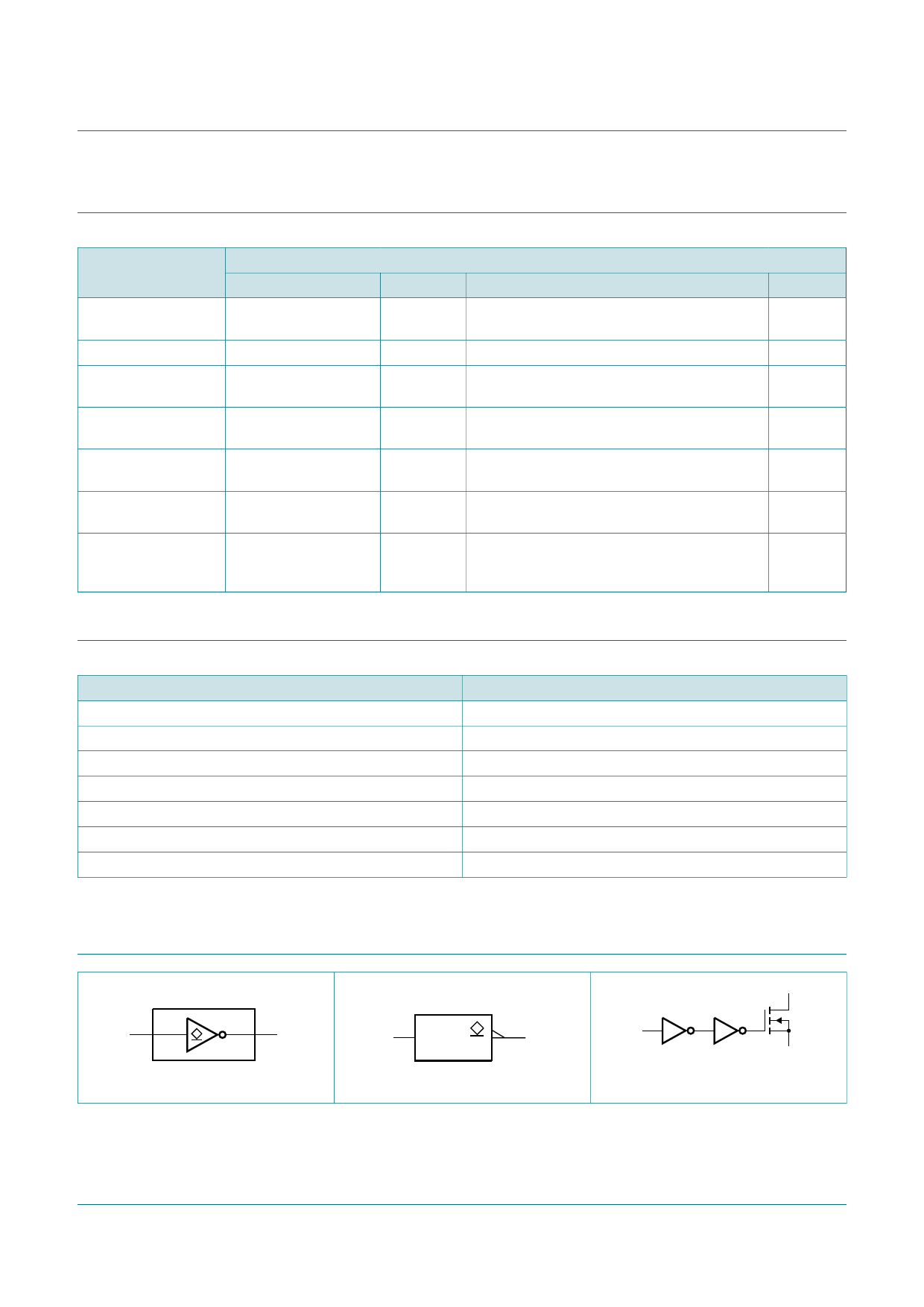
5 Functional diagram
Y
2A
Y4
mna618
Figure 1. Logic symbol
A2
4Y
mna619
Figure 2. IEC logic symbol
A
GND
mna620
Figure 3. Logic diagram
74LVC1G06
Product data sheet
All information provided in this document is subject to legal disclaimers.
Rev. 12 — 22 May 2018
© Nexperia B.V. 2018. All rights reserved.
2 / 19
Share Link: 