7549 查看數據表(PDF) - Renesas Electronics
零件编号
产品描述 (功能)
生产厂家
7549 Datasheet PDF : 86 Pages
| |||
7549 Group
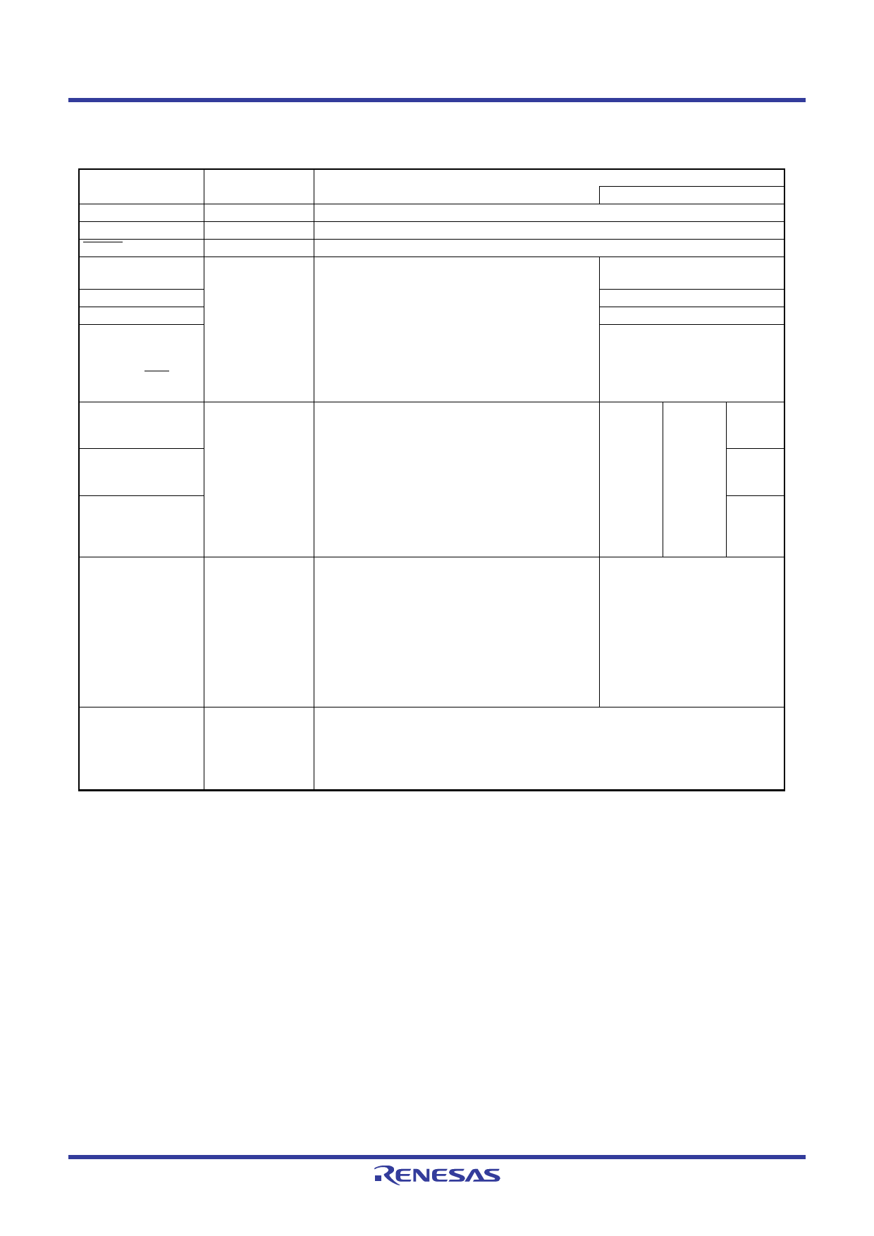
PIN DESCRIPTION
Table 2 Pin description
Pin
Name
Function
Function except a port function
VCC,VSS
Power source
Apply voltage of 1.8 to 5.5 V to Vcc, and 0 V to Vss.
CNVSS
CNVSS
Controls the operation mode of the chip. Connected to VSS.
RESET
Reset input
Reset input pin for active “L”
P00(LED0)/INT0
P01(LED1)/INT1
P02(LED2)
P03(LED3)/CAP0
I/O port P0
•8-bit I/O port.
•I/O direction register allows each pin to be individu-
ally programmed as either input or output.
•CMOS compatible input level
Interrupt input pin
Capture input pin
P04(LED4)/RXD
P05(LED5)/TXD
P06(LED6)/SCLK
P07(LED7)/SRDY
•CMOS 3-state output structure
Serial interface function pin
•Whether a built-in pull-up resistor is to be used or not
can be determined by program.
•High drive capacity for LED drive port can be
selected by program.
P10/AN0/KEY0/CMP0
P11/AN1/KEY1/CMP1
P12/AN2/KEY2/CMP2
P13/AN3/KEY3/T2OUT
I/O port P1
P14/AN4/KEY4
P15/AN5/KEY5
P16/AN6/KEY6
P17/AN7/KEY7
•8-bit I/O port.
•I/O direction register allows each pin to be individu-
ally programmed as either input or output.
•CMOS compatible input level
•CMOS 3-state output structure
•Whether a built-in pull-up resistor is to be used or not
can be determined by program.
Input pins
for A/D
converter
Key-input
(key-on
wake up
interrupt
input) pin
Compare
output
pin
Timer 2
output
pin
P20/XOUT/XCOUT
I/O port P2
P21/XIN/XCIN (Note)
•2-bit I/O port. (P20/XOUT/XCOUT is only for output)
•I/O direction register allows each pin to be individu-
ally programmed as either input or output.
•CMOS compatible input level
•CMOS 3-state output structure
•Function set ROM allows pins to be used as clock
pins.
Pins XIN and XOUT, or pins XCIN
and XCOUT, can be used as clock
pins by connecting a ceramic
resonator, crystal oscillator, or 32
kHz crystal oscillator between
them. Alternately, an external
clock may be input to the
P20/XOUT/XCOUT pin. In this case,
the P21/XIN/XCIN pin can be used
as an I/O port.
P30, P31
I/O port P3
•2-bit I/O port.
•I/O direction register allows each pin to be individually programmed as either input or
output.
•CMOS compatible input level
•CMOS 3-state output structure
NOTE:
1. The oscillation circuit is built in the P20/XOUT/XCOUT pin and the P21/XIN/XCIN pin. When the Vcc of the microcomputer is lower than
the operation lower bound voltage even if these pins are used as I/O ports, the oscillation circuit is connected and undefined values
may be output from these pins.
Rev.2.02 Mar 31, 2009 Page 6 of 81
REJ03B0202-0202
Share Link: 