EDI88130LPS17CB 查看數據表(PDF) - White Electronic Designs => Micro Semi
零件编号
产品描述 (功能)
生产厂家
EDI88130LPS17CB Datasheet PDF : 9 Pages
| |||
White Electronic Designs
EDI88130CS
ABSOLUTE MAXIMUM RATINGS
Parameter
Unit
Voltage on any pin relative to VSS
-0.2 to 7.0
V
Operating Temperature TA (Ambient)
Industrial
-40 to +85
°C
Military
-55 to +125
°C
Storage Temperature, Ceramic
-65 to +150
°C
Power Dissipation
1.7
W
Output Current
40
mA
Junction Temperature, TJ
175
°C
NOTE:
Stress greater than those listed under "Absolute Maximum Ratings" may cause
permanent damage to the device. This is a stress rating only and functional operation
of the device at these or any other conditions greater than those indicated in the
operational sections of this specification is not implied. Exposure to absolute maximum
rating conditions for extended periods may affect reliability.
RECOMMENDED OPERATING CONDITIONS
Parameter
Symbol Min
Supply Voltage
VCC
4.5
Supply Voltage
VSS
0
Input High Voltage
VIH
2.2
Input Low Voltage
VIL
-0.5
Typ Max Unit
5.0
5.5
V
0
0
V
— VCC +0.5 V
—
+0.8
V
TRUTH TABLE
OE# CS1# CS2
XHX
XXL
HLH
L LH
XLH
WE#
Mode
X
Standby
X
Standby
H Output Deselect
H
Read
L
Write
Output
High Z
High Z
High Z
Data Out
Data In
Power
Icc2, Icc3
Icc2, Icc3
Icc1
Icc1
Icc1
CAPACITANCE
TA = +25°C
Parameter Symbol
Condition
Address Lines CI
Data Lines
CO
VIN = Vcc or Vss,
f = 1.0MHz
VOUT = Vcc or Vss,
f = 1.0MHz
These parameters are sampled, not 100% tested.
Max
LCC
CSOJ,DIP,
Flatpack
Unit
6 12 pF
8 14 pF
Parameter
Input Leakage Current
Output Leakage Current
Operating Power Supply Current
Standby (TTL) Power Supply Current
Full Standby Power Supply Current
Output Low Voltage
Output High Voltage
DC CHARACTERISTICS
VCC = 5.0V, -55°C ≤ TA ≤ +125°C
Symbol
ILI
ILO
Conditions
VIN = 0V to VCC
VI/O = 0V to VCC
Icc1 WE#, CS1# = VIL, II/O = 0mA, CS2 = VIH
Icc2
CS1# ≥ VIH and/or CS2 ≤ VIL,
VIN ≥ VIH or ≤ VIL
Icc3 CS1# ≥ VCC -0.2V and/or CS2 ≤ 0.2V
VIN ≥ VCC -0.2V or VIN ≤ 0.2V
VOL IOL = 8.0mA
VOH IOH = -4.0mA
Min Typ Max Units
— — ±5 µA
— — ±10 µA
(15-17ns) —
300 mA
(20ns) —
225 mA
(25-55ns) —
200 mA
(17-55ns) —
25 mA
(15ns) —
60 mA
CS (17-55ns) —
3
10 mA
CS (15ns) — — 15 mA
LPS — —
5 mA
— — 0.4 V
2.4 —
—
V
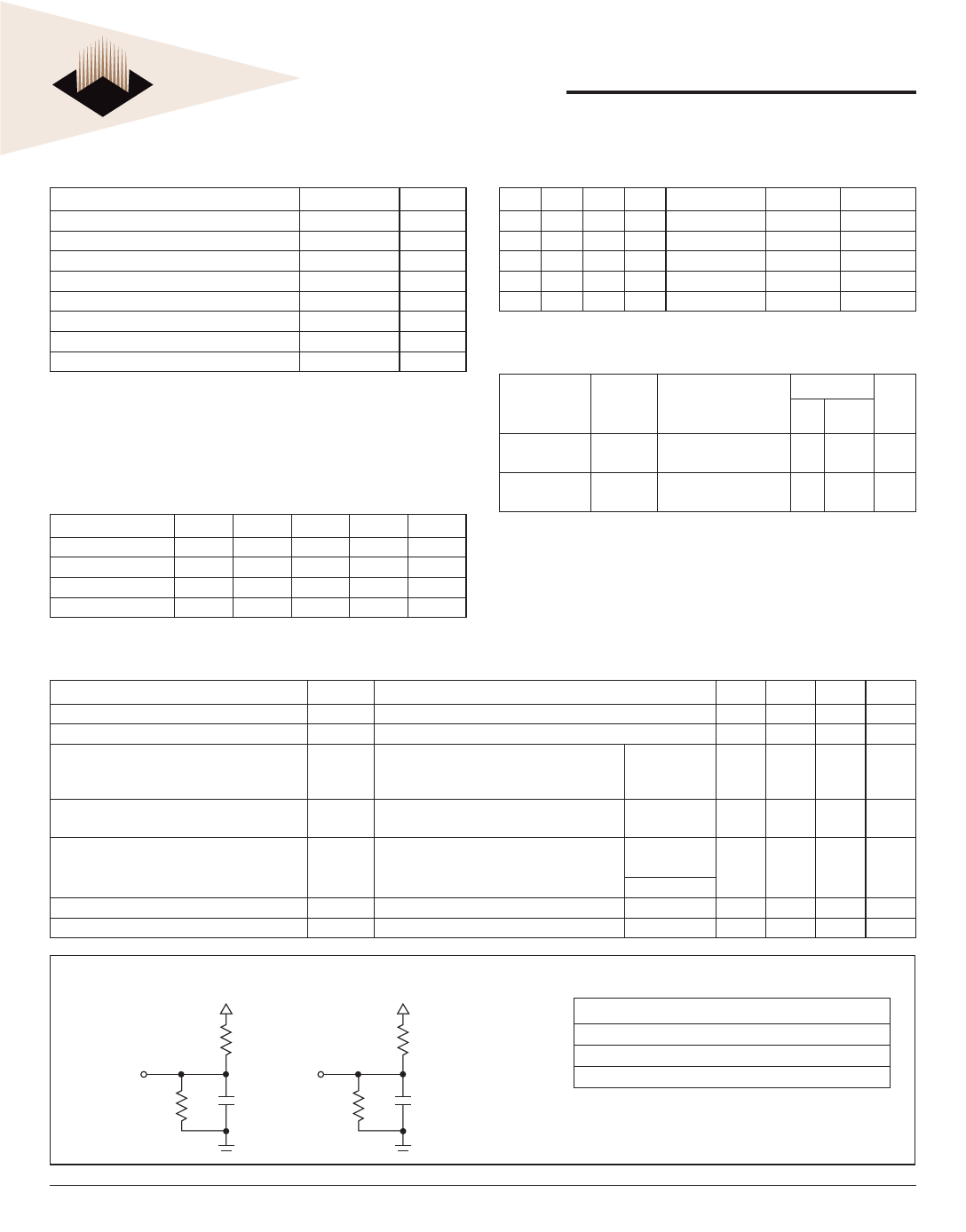
AC Test Conditions
Figure 1
Vcc
480Ω
Q
255Ω
30pF
Figure 2
Q
255Ω
Vcc
480Ω
5pF
Input Pulse Levels
VSS to 3.0V
Input Rise and Fall Times
Input and Output Timing Levels
Output Load
5ns
1.5V
Figure 1
NOTE: For tEHQZ, tGHQZ and tWLQZ, CL = 5pF Figure 2
White Electronic Designs Corp. reserves the right to change products or specifications without notice.
March 2002
Rev. 11
2
White Electronic Designs Corporation • (602) 437-1520 • www.wedc.com
Share Link: 