AD5123 查看數據表(PDF) - Analog Devices
零件编号
产品描述 (功能)
生产厂家
AD5123 Datasheet PDF : 28 Pages
| |||
Data Sheet
AD5123/AD5143
INTERFACE TIMING SPECIFICATIONS
VDD = 2.3 V to 5.5 V; all specifications TMIN to TMAX, unless otherwise noted.
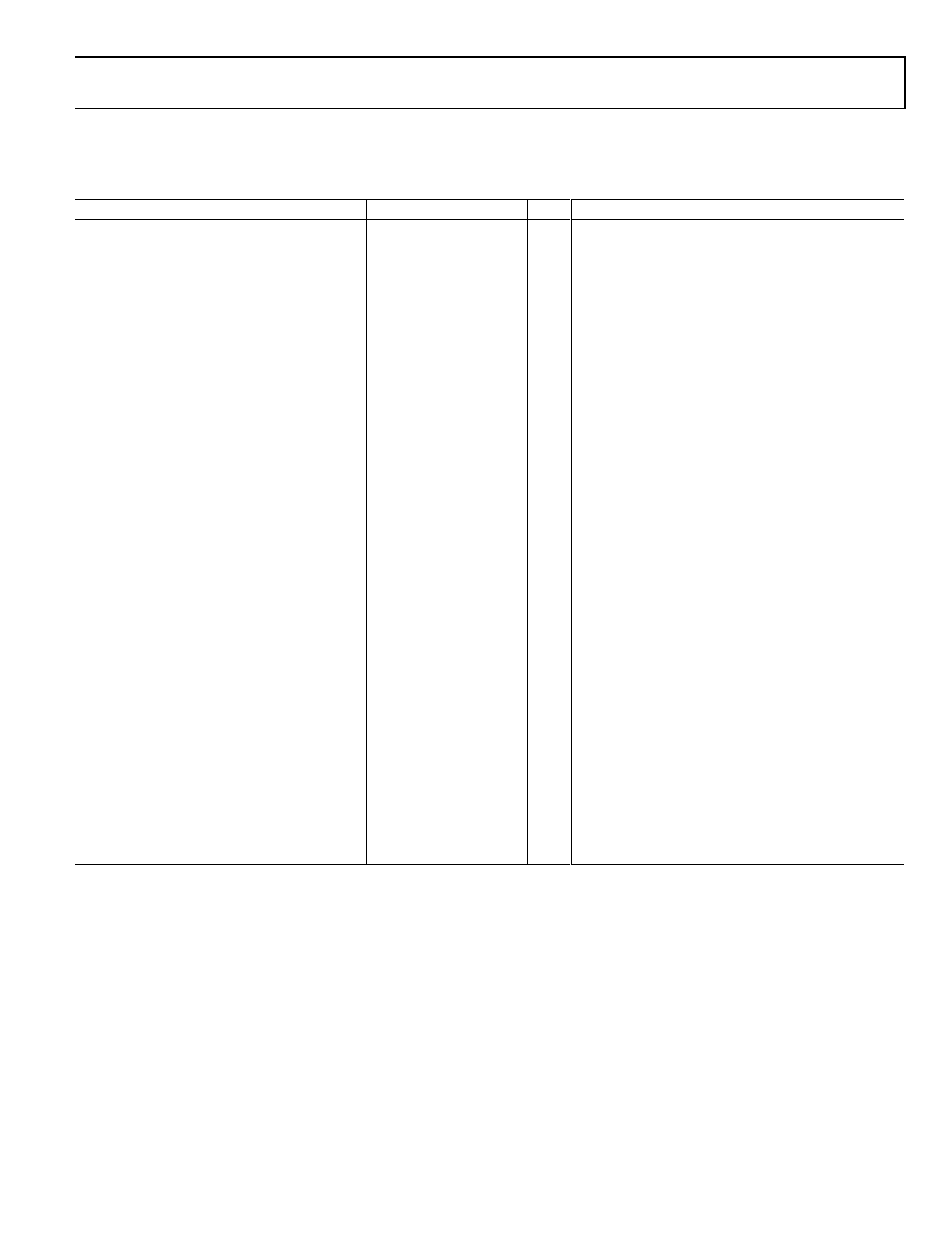
Table 4. I2C Interface
Parameter1 Test Conditions/Comments Min
Typ Max Unit Description
fSCL2
Standard mode
100 kHz Serial clock frequency
Fast mode
400 kHz
t1
Standard mode
4.0
µs SCL high time, tHIGH
Fast mode
0.6
µs
t2
Standard mode
4.7
µs SCL low time, tLOW
Fast mode
1.3
µs
t3
Standard mode
250
ns Data setup time, tSU; DAT
Fast mode
100
ns
t4
Standard mode
0
3.45 µs Data hold time, tHD; DAT
Fast mode
0
0.9 µs
t5
Standard mode
4.7
µs Setup time for a repeated start condition, tSU; STA
Fast mode
0.6
µs
t6
Standard mode
4
µs Hold time (repeated) for a start condition, tHD; STA
Fast mode
0.6
µs
t7
Standard mode
4.7
µs Bus free time between a stop and a start condition, tBUF
Fast mode
1.3
µs
t8
Standard mode
4
µs Setup time for a stop condition, tSU; STO
Fast mode
0.6
µs
t9
Standard mode
1000 ns Rise time of SDA signal, tRDA
Fast mode
20 + 0.1 CL
300 ns
t10
Standard mode
300 ns Fall time of SDA signal, tFDA
Fast mode
20 + 0.1 CL
300 ns
t11
Standard mode
1000 ns Rise time of SCL signal, tRCL
Fast mode
20 + 0.1 CL
300 ns
t11A
Standard mode
1000 ns
Rise time of SCL signal after a repeated start condition
and after an acknowledge bit, tRCL1 (not shown in Figure 3)
Fast mode
20 + 0.1 CL
300 ns
t12
Standard mode
300 ns Fall time of SCL signal, tFCL
Fast mode
20 + 0.1 CL
300 ns
tSP3
Fast mode
0
50 ns Pulse width of suppressed spike (not shown in Figure 3)
tEEPROM_PROGRAM4
15 50 ms Memory program time (not shown in Figure 3)
tEEPROM_READBACK
tPOWER_UP5
7 30 µs Memory readback time (not shown in Figure 3)
75 µs Power-on EEPROM restore time (not shown in Figure 3)
tRESET
30
µs Reset EEPROM restore time (not shown in Figure 3)
1 Maximum bus capacitance is limited to 400 pF.
2 The SDA and SCL timing is measured with the input filters enabled. Switching off the input filters improves the transfer rate; however, it has a negative effect on the
EMC behavior of the part.
3 Input filtering on the SCL and SDA inputs suppresses noise spikes that are less than 50 ns for fast mode.
4 EEPROM program time depends on the temperature and EEPROM write cycles. Higher timing is expected at lower temperatures and higher write cycles.
5 Maximum time after VDD − VSS is equal to 2.3 V.
Rev. A | Page 9 of 28
Share Link: 