AD5242 查看數據表(PDF) - Analog Devices
零件编号
产品描述 (功能)
生产厂家
AD5242 Datasheet PDF : 20 Pages
| |||
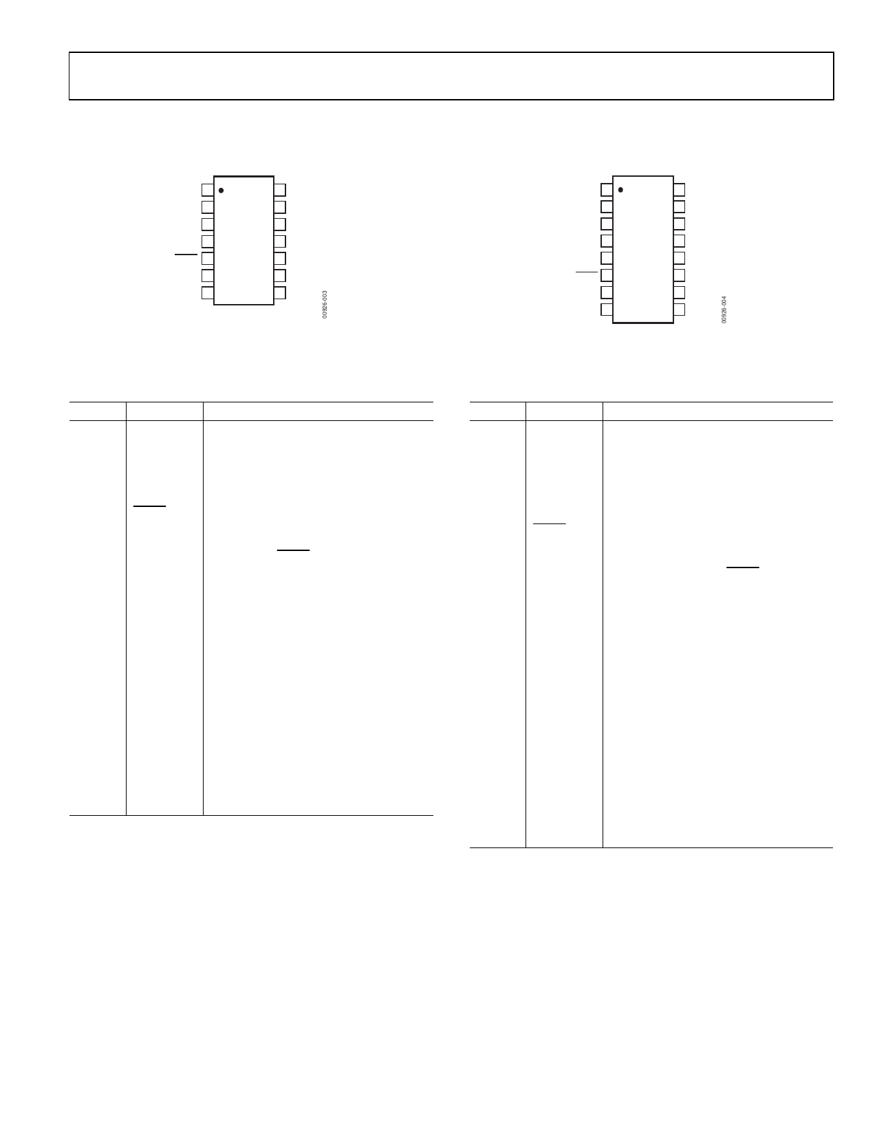
PIN CONFIGURATIONS AND FUNCTION DESCRIPTIONS
AD5241/AD5242
A1 1
14 O1
W1 2
13 NC
B1
VDD
SHDN
3 AD5241 12 O2
4 TOP VIEW 11 VSS
5 (Not to Scale) 10 DGND
SCL 6
9 AD1
SDA 7
8 AD0
NC = NO CONNECT
Figure 6. AD5241 Pin Configuration
Table 4. AD5241 Pin Function Descriptions
Pin No. Mnemonic Description
1
A1
Resistor Terminal A1.
2
W1
Wiper Terminal W1.
3
B1
Resistor Terminal B1.
4
VDD
Positive Power Supply, Specified for
Operation from 2.2 V to 5.5 V.
5
SHDN
Active low, asynchronous connection of
Wiper W to Terminal B, and open circuit
of Terminal A. RDAC register contents
unchanged. SHDN should tie to VDD
if not used.
6
SCL
Serial Clock Input.
7
SDA
Serial Data Input/Output.
8
AD0
Programmable Address Bit for Multiple
Package Decoding. Bit AD0 and Bit AD1
provide four possible addresses.
9
AD1
Programmable Address Bit for Multiple
Package Decoding. Bit AD0 and Bit AD1
provide four possible addresses.
10
DGND
Common Ground.
11
VSS
Negative Power Supply, Specified for
Operation from 0 V to −2.7 V.
12
O2
Logic Output Terminal O2.
13
NC
No Connect.
14
O1
Logic Output Terminal O1.
O1 1
A1 2
16 A2
15 W2
W1 3
14 B2
B1 4 AD5242 13 O2
TOP VIEW
VDD 5 (Not to Scale) 12 VSS
SHDN 6
11 DGND
SCL 7
10 AD1
SDA 8
9 AD0
Figure 7. AD5242 Pin Configuration
Table 5. AD5242 Pin Function Descriptions
Pin No. Mnemonic Description
1
O1
Logic Output Terminal O1.
2
A1
Resistor Terminal A1.
3
W1
Wiper Terminal W1.
4
B1
Resistor Terminal B1.
5
VDD
Positive Power Supply, Specified for
Operation from 2.2 V to 5.5 V.
6
SHDN
Active Low, Asynchronous Connection
of Wiper W to Terminal B, and Open
Circuit of Terminal A. RDAC register
contents unchanged. SHDN should
tie to VDD, if not used.
7
SCL
Serial Clock Input.
8
SDA
Serial Data Input/Output.
9
AD0
Programmable Address Bit for Multiple
Package Decoding. Bit AD0 and Bit AD1
provide four possible addresses.
10
AD1
Programmable Address Bit for Multiple
Package Decoding. Bit AD0 and Bit AD1
provide four possible addresses.
11
DGND
Common Ground.
12
VSS
Negative Power Supply, Specified for
Operation from 0 V to −2.7 V.
13
O2
Logic Output Terminal O2.
14
B2
Resistor Terminal B2.
15
W2
Wiper Terminal W2.
16
A2
Resistor Terminal A2.
Rev. C | Page 7 of 20
Share Link: 