AD5245 查看數據表(PDF) - Analog Devices
零件编号
产品描述 (功能)
生产厂家
AD5245 Datasheet PDF : 20 Pages
| |||
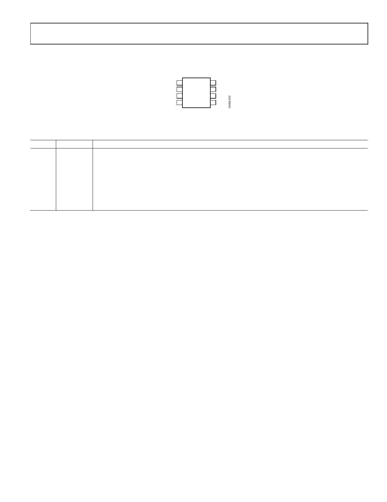
PIN CONFIGURATION AND FUNCTION DESCRIPTIONS
W1
8A
VDD 2 AD5245 7 B
GND 3 TOP VIEW 6 AD0
(Not to Scale)
SCL 4
5 SDA
Figure 3. Pin Configuration
Table 5. Pin Function Descriptions
Pin No. Mnemonic Description
1
W
W Terminal. GND ≤ VW ≤ VDD.
2
VDD
Positive Power Supply.
3
GND
Digital Ground.
4
SCL
Serial Clock Input. Positive edge triggered. Pull-up resistor required.
5
SDA
Serial Data Input/Output. Pull-up resistor required.
6
AD0
Programmable Address Bit 0 for Two-Device Decoding.
7
B
B Terminal. GND ≤ VB ≤ VDD.
8
A
A Terminal. GND ≤ VA ≤ VDD.
AD5245
Rev. B | Page 7 of 20
Share Link: 