AD524CDZ 查看數據表(PDF) - Analog Devices
零件编号
产品描述 (功能)
生产厂家
AD524CDZ Datasheet PDF : 28 Pages
| |||
AD524
ABSOLUTE MAXIMUM RATINGS
Table 3.
Parameter
Supply Voltage
Internal Power Dissipation
Input Voltage1
(Either Input Simultaneously) |VIN| + |VS|
Output Short-Circuit Duration
Storage Temperature Range
(R)
(D, E)
Operating Temperature Range
AD524A/AD524B/AD524C
AD524S
Lead Temperature (Soldering, 60 sec)
Rating
±18 V
450 mW
<36 V
Indefinite
–65°C to +125°C
–65°C to +150°C
–25°C to +85°C
–55°C to +125°C
+300°C
1 Maximum input voltage specification refers to maximum voltage to which
either input terminal may be raised with or without device power applied.
For example, with ±18 volt supplies maximum, VIN is ±18 V; with zero supply
voltage maximum, VIN is ±36 V.
Stresses above those listed under Absolute Maximum Ratings
may cause permanent damage to the device. This is a stress
rating only; functional operation of the device at these or any
other conditions above those indicated in the operational
section of this specification is not implied. Exposure to absolute
maximum rating conditions for extended periods may affect
device reliability.
OUTPUT
NULL
14
OUTPUT
NULL
15
G = 10
13
G = 100
12
G = 1000
11
RG1 16
SENSE
10
9
OUTPUT
8 +VS
–INPUT
1
+INPUT
2
RG2
3
4
INPUT
NULL
5
INPUT
NULL
6
REFERENCE
0.170 (4.33)
PAD NUMBERS CORRESPOND TO PIN NUMBERS FOR
THE D-16 AND RW-16 16-LEAD CERAMIC PACKAGES.
Figure 2. Metallization Photograph
Contact factory for latest dimensions;
Dimensions shown in inches and (mm)
0.103
(2.61)
7 –VS
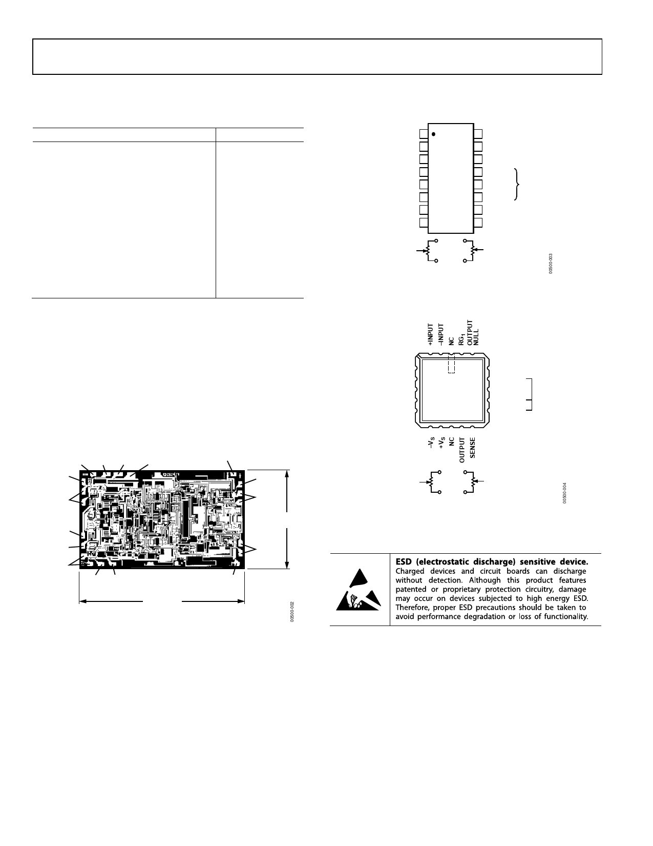
CONNECTION DIAGRAMS
– INPUT 1
16 RG1
+ INPUT 2
15 OUTPUT NULL
RG2 3
14 OUTPUT NULL
INPUT NULL 4 AD524 13 G = 10
INPUT NULL
5
TOP VIEW
(Not to Scale)
12
G = 100
REFERENCE 6
11 G = 1000
SHORT TO
RG2 FOR
DESIRED
GAIN
–VS 7
10 SENSE
+VS 8
9 OUTPUT
+VS
INPUT
OFFSET NULL
4 15
5 14
–VS
OUTPUT
OFFSET NULL
Figure 3. Ceramic (D) and
SOIC (RW-16 and D-16) Packages
RG2 4
INPUT NULL 5
NC 6
INPUT NULL 7
REFERENCE 8
3 2 1 20 19
AD524
TOP VIEW
(Not to Scale)
18 OUTPUT NULL
17 G = 10
16 NC
15 G = 100
14 G = 1000
SHORT TO
RG2 FOR
DESIRED
GAIN
NC = NO CONNECT 9 10 11 12 13
+VS
INPUT
OFFSET NULL
7 19
5 18
–VS
OUTPUT
OFFSET NULL
Figure 4. Leadless Chip Carrier (E)
ESD CAUTION
Rev. F | Page 8 of 28
Share Link: 