AD5255BRU25-RL7 查看數據表(PDF) - Analog Devices
零件编号
产品描述 (功能)
生产厂家
AD5255BRU25-RL7 Datasheet PDF : 20 Pages
| |||
AD5255
Parameter
DIGITAL INPUTS AND OUTPUTS
Input Logic High
Symbol
VIH
Input Logic Low
VIL
Output Logic High (SDA)
VOH
Output Logic Low
VOL
WP Leakage Current
A0 Leakage Current
Input Leakage Current (Excluding WPand A0)
Input Capacitance5
POWER SUPPLIES
Single-Supply Power Range
Dual-Supply Power Range
IWP
IA0
II
CI
VDD
VDD/VSS
Positive Supply Current
IDD
Negative Supply Current
ISS
EEMEM Data Storing Mode Current
EEMEM Data Restoring Mode Current
Power Dissipation7
Power Supply Sensitivity5
IDD_STORE
IDD_RESTORE
PDISS
PSS
Conditions
Min Typ1 Max Unit
VDD = 5 V, VSS = 0 V
VDD/VSS = +2.7 V/0 V or
VDD/VSS = ±2.5 V
VDD = 5 V, VSS = 0 V
VDD/VSS = +2.7 V/0 V or
VDD/VSS = ±2.5 V
RPULL-UP = 2.2 kΩ to VDD = 5 V,
VSS = 0 V
RPULL-UP = 2.2 kΩ to VDD = 5 V,
VSS = 0 V
WP = VDD
A0 = GND
VIN = 0 V or VDD
2.4
2.1
4.9
5
V
V
0.8 V
0.6 V
V
0.4 V
9
μA
3
μA
±1 μA
pF
VSS = 0 V
2.7
5.5 V
±2.2
±2.7 V
5
5
VIH = VDD or VIL = GND, VSS = 0 V
5
15 μA
VIH = VDD or VIL = GND,
VDD = 2.5 V, VSS = −2.5 V
−5 −15 μA
VIH = VDD or VIL = GND
35
mA
VIH = VDD or VIL = GND
2.5
mA
VIH = VDD = 5 V or VIL = GND
25 75 μW
∆VDD = 5 V ± 10%
0.01 0.025 %/%
1 Typical represents average readings at 25°C, VDD = 5 V.
2 Resistor position nonlinearity error, R-INL, is the deviation from an ideal value measured between the maximum resistance and the minimum resistance wiper
positions. R-DNL measures the relative step change from ideal between successive tap positions.
3 INL and DNL are measured at VW with the RDAC configured as a potentiometer divider similar to a voltage output DAC. VA = VDD and VB = 0 V.
4 Resistor Terminals A, B, W have no limitations on polarity with respect to each other.
5 Guaranteed by design and not subject to production test.
6 Bandwidth, noise, and settling time are dependent on the terminal resistance value chosen. The lowest R value results in the fastest settling time and highest
bandwidth. The highest R value results in the minimum overall power consumption.
7 PDISS is calculated from (IDD × VDD). CMOS logic level inputs result in minimum power dissipation.
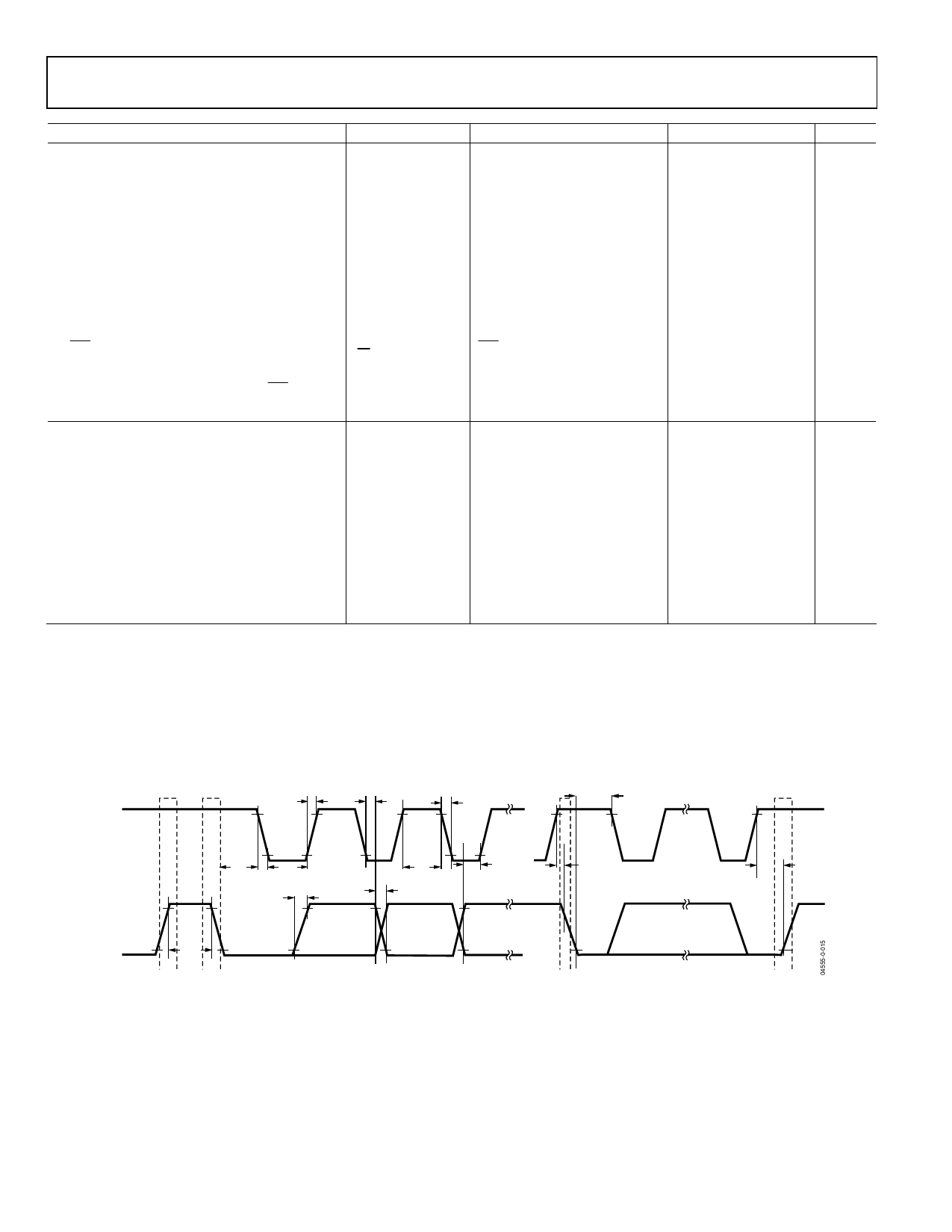
t8
t6
t9
t2
SCL
t2
t3
t4
t7
t5
t8
t9
SDA
t1
P
S
S
Figure 2. I2C Timing Diagram
t10
P
Rev. A | Page 4 of 20
Share Link: 