AD5247 查看數據表(PDF) - Analog Devices
零件编号
产品描述 (功能)
生产厂家
AD5247 Datasheet PDF : 20 Pages
| |||
Data Sheet
AD5247
Parameter
DYNAMIC CHARACTERISTICS6, 8
Bandwidth –3 dB
Total Harmonic Distortion
VW Settling Time (10 kΩ/50 kΩ/100 kΩ)
Resistor Noise Voltage Density
Symbol Conditions
BW
THDW
tS
eN_WB
RAB = 10 kΩ/50 kΩ/100 kΩ,
code = 0x40
VA =1 V rms, f = 1 kHz, RAB = 10 kΩ
VA = 5 V ±1 LSB error band
RWB = 5 kΩ, RS = 0
Min Typ1
Max Unit
600/100/40
0.05
2
9
kHz
%
µs
nV/√Hz
1 Typical specifications represent average readings at 25°C and VDD = 5 V.
2 Resistor position nonlinearity error R-INL is the deviation from an ideal value measured between the maximum resistance and the minimum resistance wiper
positions. R-DNL measures the relative step change from ideal between successive tap positions. Parts are guaranteed monotonic.
3 VA = VDD, wiper (VW) = no connect.
4 INL and DNL are measured at VW, with the RDAC configured as a potentiometer divider similar to a voltage output DAC. VA = VDD and VB = 0 V.
DNL specification limits of ±1 LSB maximum are guaranteed monotonic operating conditions.
5 Resistor Terminal A and Resistor Terminal W have no limitations on polarity with respect to each other.
6 Guaranteed by design, not subject to production test.
7 PDISS is calculated from (IDD × VDD). CMOS logic level inputs result in minimum power dissipation.
8 All dynamic characteristics use VDD = 5 V.
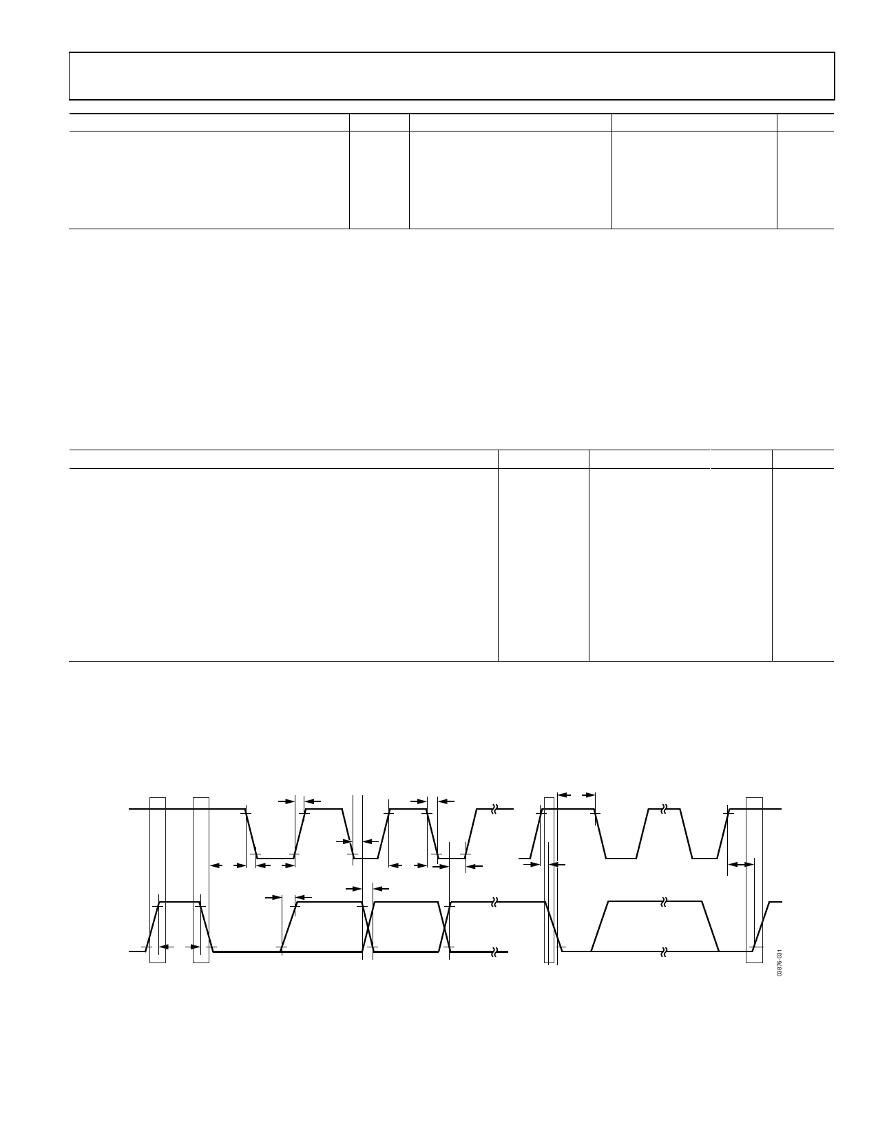
TIMING CHARACTERISTICS—5 kΩ, 10 kΩ, 50 kΩ, AND 100 kΩ VERSIONS
VDD = 5 V ± 10% or 3 V ± 10%, VA = VDD, −40°C < TA < +125°C, unless otherwise noted.
Table 3.
Parameter1, 2, 3
SCL Clock Frequency
Bus Free Time Between Stop and Start, tBUF
Hold Time (Repeated Start), tHD;STA5
Low Period of SCL Clock, tLOW
High Period of SCL Clock, tHIGH
Setup Time for Repeated Start Condition, tSU;STA
Data Hold Time, tHD;DAT
Data Setup Time, tSU;DAT
Fall Time of Both SDA and SCL Signals, tF
Rise Time of Both SDA and SCL Signals, tR
Setup Time for Stop Condition, tSU;STO
Symbol
Min
fSCL
t1
1.3
t2
0.6
t3
1.3
t4
0.6
t5
0.6
t6
t7
100
t8
t9
t10
0.6
1 Specifications apply to all parts.
2 Guaranteed by design, not subject to production test.
3 See timing diagrams (Figure 2, Figure 33, and Figure 34) for locations of measured values.
4 Typical specifications represent average readings at 25°C and VDD = 5 V.
5 After this period, the first clock pulse is generated.
Typ 4
Max
400
50
0.9
300
300
Unit
kHz
µs
µs
µs
µs
µs
µs
ns
ns
ns
µs
SCL
t2
SDA
t1
P
S
t8
t9
t6
t3
t9
t8
t4
t7
t2
t5
S
Figure 2. I2C Interface, Detailed Timing Diagram
t10
P
Rev. F | Page 5 of 20
Share Link: 