AD5697R жҹҘзңӢж•ёж“ҡиЎЁпјҲPDFпјү - Analog Devices
йӣ¶д»¶зј–еҸ·
дә§е“ҒжҸҸиҝ° (еҠҹиғҪ)
з”ҹдә§еҺӮ家
AD5697R Datasheet PDF : 27 Pages
| |||
AD5697R
Data Sheet
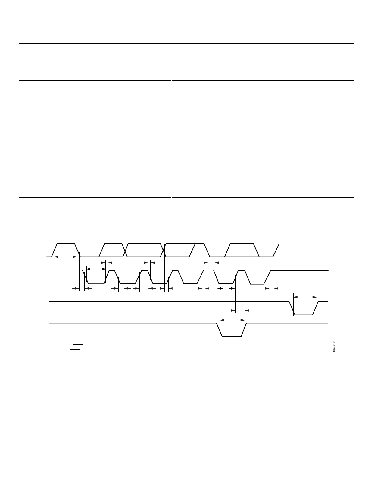
TIMING CHARACTERISTICS
VDD = 2.7 V to 5.5 V; 1.62 V вүӨ VLOGIC вүӨ 5.5 V; all specifications TMIN to TMAX, unless otherwise noted. See Figure 2.
Table 4.
Parameter1
t1
t2
t3
t4
t5
t6 2
t7
t8
t9
t10
t11
t12
t13
CB3
Min
2.5
0.6
1.3
0.6
100
0
0.6
0.6
1.3
0
20 + 0.1CB3
20
400
Max
0.9
300
300
400
Unit
Вөs
Вөs
Вөs
Вөs
ns
Вөs
Вөs
Вөs
Вөs
ns
ns
ns
ns
pF
Test Conditions/Comments
SCL cycle time
SCL high time, tHIGH
SCL low time, tLOW
Start/repeated start condition hold time, tHD,STA
Data setup time, tSU,DAT
Data hold time, tHD,DAT
Setup time for repeated start, tSU,STA
Stop condition setup time, tSU,STO
Bus free time between a stop and a start condition, tBUF
Rise time of SCL and SDA when receiving, tR
Fall time of SDA and SCL when transmitting/receiving, tF
LDAC pulse width
SCL rising edge to LDAC rising edge
Capacitive load for each bus line
1 Guaranteed by design and characterization; not production tested.
2 A master device must provide a hold time of at least 300 ns for the SDA signal (referred to the VIH minimum of the SCL signal) to bridge the undefined region of the
falling edge of the SCL.
3 CB is the total capacitance of one bus line in pF. tR and tF measured between 0.3 VDD and 0.7 VDD.
START
CONDITION
SDA
SCL
t9
t10
t3
t4
t6
LDAC1
LDAC2
NOTES
1ASYNCHRONOUS LDAC UPDATE MODE.
2SYNCHRONOUS LDAC UPDATE MODE.
REPEATED START
CONDITION
t11
t4
t2
t5
t1
t7
t13
t12
Figure 2. 2-Wire Serial Interface Timing Diagram
STOP
CONDITION
t8
t12
Rev. B | Page 6 of 27
Share Link: 