AD5697R жҹҘзңӢж•ёж“ҡиЎЁпјҲPDFпјү - Analog Devices
йӣ¶д»¶зј–еҸ·
дә§е“ҒжҸҸиҝ° (еҠҹиғҪ)
з”ҹдә§еҺӮ家
AD5697R Datasheet PDF : 27 Pages
| |||
AD5697R
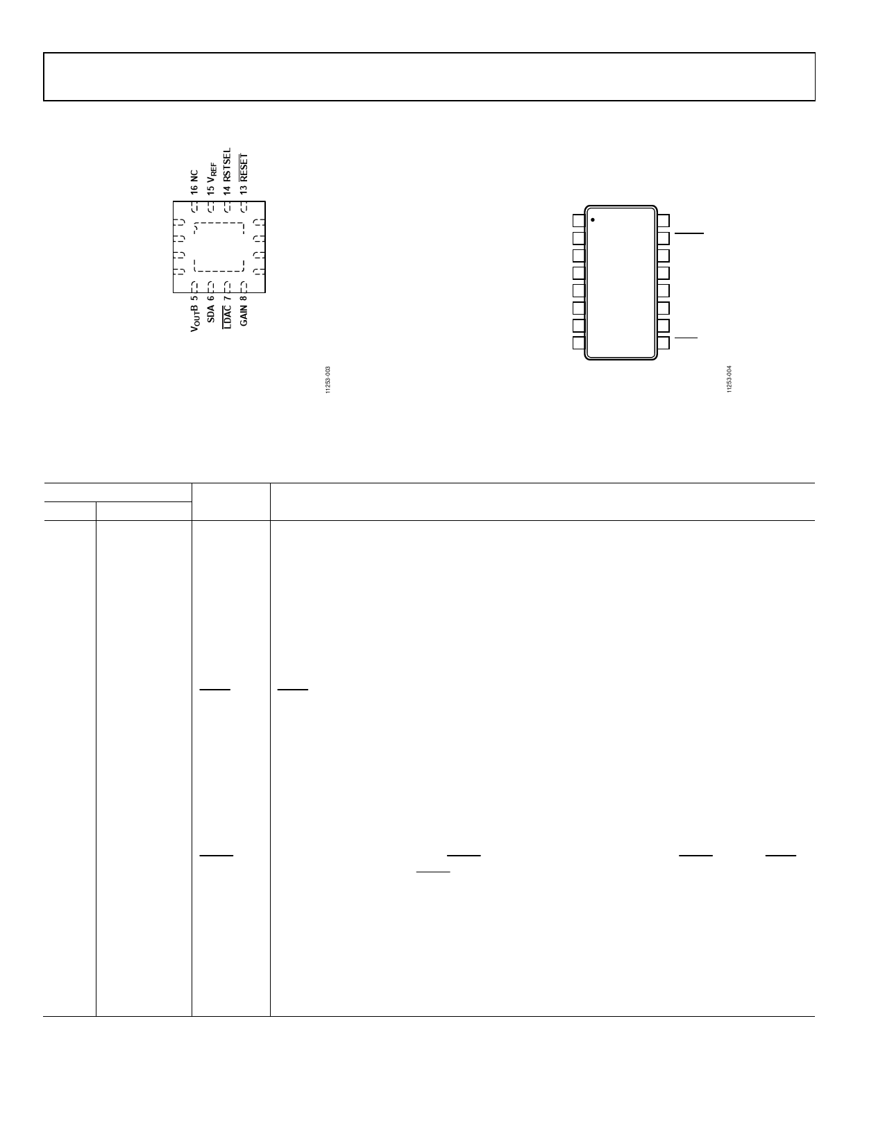
PIN CONFIGURATIONS AND FUNCTION DESCRIPTIONS
Data Sheet
VOUTA 1
GND 2
VDD 3
NC 4
AD5697R
12 A1
11 SCL
10 A0
9 VLOGIC
TOP VIEW
(Not to Scale)
NOTES
1. THE EXPOSED PAD MUST BE TIED TO GND.
2. NC = NO CONNECT. DO NOT CONNECT TO
THIS PIN.
Figure 3. 16-Lead LFCSP Pin Configuration
VREF 1
NC 2
VOUTA 3
GND 4
VDD 5
NC 6
VOUTB 7
SDA 8
16 RSTSEL
15 RESET
AD5697R
TOP VIEW
(Not to Scale)
14 A1
13 SCL
12 A0
11 VLOGIC
10 GAIN
9 LDAC
NOTES
1. NC = NO CONNECT. DO NOT CONNECT TO
THIS PIN.
Figure 4. 16-Lead TSSOP Pin Configuration
Table 6. Pin Function Descriptions
Pin No.
LFCSP TSSOP
Mnemonic
1
3
VOUTA
16
2
NC
2
4
GND
3
5
VDD
4
6
5
7
6
8
NC
VOUTB
SDA
7
9
LDAC
8
10
9
11
10
12
11
13
12
14
13
15
GAIN
VLOGIC
A0
SCL
A1
RESET
14
16
15
1
RSTSEL
VREF
17
Not applicable EPAD
Description
Analog Output Voltage from DAC A. The output amplifier has rail-to-rail operation.
No Connect. Do not connect to this pin.
Ground Reference Point for All Circuitry on the Part.
Power Supply Input. This part can be operated from 2.7 V to 5.5 V. Decouple the supply with a
10 ОјF capacitor in parallel with a 0.1 ОјF capacitor to GND.
No Connect. Do not connect to this pin.
Analog Output Voltage from DAC B. The output amplifier has rail-to-rail operation.
Serial Data Input. This pin is used in conjunction with the SCL line to clock data into or out of the
24-bit input shift register. SDA is a bidirectional, open-drain data line that should be pulled to the
supply with an external pull-up resistor.
LDAC can be operated in two modes, asynchronous and synchronous. Pulsing this pin low allows
either or both DAC registers to be updated if the input registers have new data. This allows both DAC
outputs to simultaneously update. This pin can also be tied permanently low.
Gain Select. When this pin is tied to GND, both DAC outputs have a span from 0 V to VREF. If this pin
is tied to VLOGIC, both DACs output a span of 0 V to 2 Г— VREF.
Digital Power Supply. Voltage ranges from 1.62 V to 5.5 V.
Address Input. Sets the first LSB of the 7-bit slave address.
Serial Clock Line. This is used in conjunction with the SDA line to clock data into or out of the 24-bit
input register.
Address Input. Sets the second LSB of the 7-bit slave address.
Asynchronous Reset Input. The RESET input is falling edge sensitive. When RESET is low, all LDAC
pulses are ignored. When RESET is activated, the input register and the DAC register are updated
with zero scale or midscale, depending on the state of the RSTSEL pin. If the pin is forced low at
power-up, the POR circuit does not initialize correctly until the pin is released.
Power-On Reset Select. Tying this pin to GND powers up both DACs to zero scale. Tying this pin to
VLOGIC powers up both DACs to midscale.
Reference Voltage. The AD5697R has a common reference pin. When using the internal reference,
this is the reference output pin. When using an external reference, this is the reference input pin.
The default for this pin is as a reference output.
Exposed Pad. The exposed pad must be tied to GND.
Rev. B | Page 8 of 27
Share Link: 