AD585 查看數據表(PDF) - Analog Devices
零件编号
产品描述 (功能)
生产厂家
AD585 Datasheet PDF : 6 Pages
| |||
AD585
For the AD585 in particular it becomes:
S/H
Offset
(V ) =
100
0.3 pC
pF + (CEXT
)
The addition of an external hold capacitor also affects the acqui-
sition time of the AD585. The change in acquisition time with
respect to the CEXT is shown graphically in Figure 2.
HOLD MODE
In the hold mode there are two important specifications that
must be considered; feedthrough and the droop rate. Feedthrough
errors appear as an attenuated version of the input at the output
while in the hold mode. Hold-Mode feedthrough varies with fre-
quency, increasing at higher frequencies. Feedthrough is an im-
portant specification when a sample and hold follows an analog
multiplexer that switches among many different channels.
Hold-mode droop rate is the change in output voltage per unit
of time while in the hold mode. Hold-mode droop originates as
leakage from the hold capacitor, of which the major leakage
current contributors are switch leakage current and bias current.
The rate of voltage change on the capacitor dV/dT is the ratio of
the total leakage current IL to the hold capacitance CH.
Droop
Rate
=
dVOUT
dT
(Volts/Sec) =
IL ( pA)
CH ( pF )
For the AD585 in particular;
Droop
Rate
=
100
100 pA
pF + (CEXT
)
Additionally the leakage current doubles for every 10°C increase
in temperature above 25°C; therefore, the hold-mode droop rate
characteristic will also double in the same fashion. The hold-mode
droop rate can be traded-off with acquisition time to provide the
best combination of droop error and acquisition time. The tradeoff
is easily accomplished by varying the value of CEXT.
Since a sample and hold is used typically in combination with
an A/D converter, then the total droop in the output voltage has
to be less than 1/2 LSB during the period of a conversion. The
maximum allowable signal change on the input of an A/D
converter is:
∆V max =
Full -Scale Voltage
2(N +1)
Once the maximum ∆V is determined then the conversion time
of the A/D converter (TCONV) is required to calculate the maxi-
mum allowable dV/dT.
dV
dt
max
=
∆V max
T CONV
dV max
The maximum dT as shown by the previous equation is
the limit not only at 25°C but at the maximum expected operat-
ing temperature range. Therefore, over the operating temperature
range the following criteria must be met (TOPERATION –25°C)
= ∆T.
(∆T °C)
dV 25° C × 2 10°C ≤ dV max
dT
dT
HOLD-TO-SAMPLE TRANSITION
The Nyquist theorem states that a band-limited signal which is
sampled at a rate at least twice the maximum signal frequency
can be reconstructed without loss of information. This means
that a sampled data system must sample, convert and acquire
the next point at a rate at least twice the signal frequency. Thus
the maximum input frequency is equal to
( ) f MAX
=
2
1
T ACQ + TCONV
+ T AP
Where TACQ is the acquisition time of the sample-to-hold
amplifier, TAP is the maximum aperture time (small enough to
be ignored) and TCONV is the conversion time of the A/D
converter.
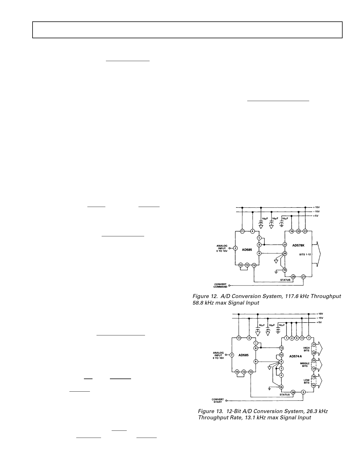
DATA ACQUISITION SYSTEMS
The fast acquisition time of the AD585 when used with a high
speed A/D converter allows accurate digitization of high fre-
quency signals and high throughput rates in multichannel data
acquisition systems. The AD585 can be used with a number of
different A/D converters to achieve high throughput rates. Fig-
ures 12 and 13 show the use of an AD585 with the AD578 and
AD574A.
Figure 12. A/D Conversion System, 117.6 kHz Throughput
58.8 kHz max Signal Input
Figure 13. 12-Bit A/D Conversion System, 26.3 kHz
Throughput Rate, 13.1 kHz max Signal Input
REV. A
–5–
Share Link: 