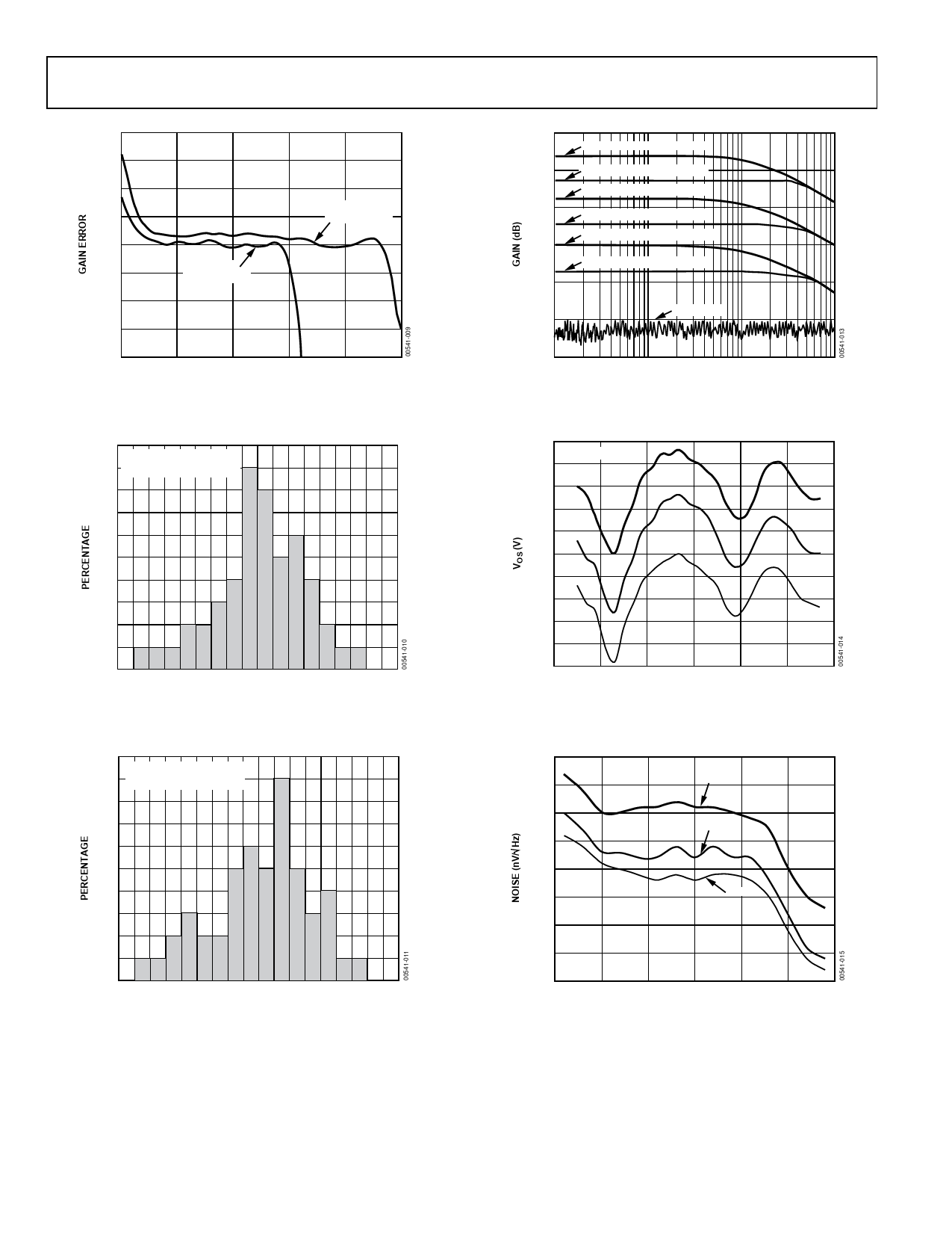
AD605(RevC) 查看數據表(PDF) - Analog Devices
零件编号
产品描述 (功能)
生产厂家
AD605 Datasheet PDF : 12 Pages
| |||
AD605
VREF
VGN
+IN
–IN
C1
VPOS
EXT
C2
VOCM
C3
EXT
R3
200k⍀
R4
200k⍀
175⍀
GAIN
CONTROL
DIFFERENTIAL
ATTENUATOR
175⍀
R2
20⍀
DISTRIBUTED GM
G1
Ao
OUT
G2
3.36k⍀
R1
820⍀
FBK
Figure 1. Simplified Block Diagram of a Single Channel of the AD605
THEORY OF OPERATION
The AD605 is a dual channel, low noise variable gain amplifier.
Figure 1 shows the simplified block diagram of one channel.
Each channel consists of a single-supply X-AMP® (hereafter
called DSX, differential single-supply X-AMP) comprised of
(a) precision passive attenuator (differential ladder)
(b) gain control block
(c) VOCM buffer with supply splitting resistors R3 and R4
(d) active feedback amplifier1 (AFA) with gain setting
resistors R1 and R2
The linear-in-dB gain response of the AD605 can generally be
described by Equation 1.
G (dB) = (Gain Scaling (dB/V)) × (Gain Control (V)) –
(19 dB – (14 dB) × (FB))
(1)
where FB = 0 if FBK-to-OUT are shorted,
FB = 1 if FBK-to-OUT is open.
Each channel provides between –14 dB to +34.4 dB through
0 dB to +48.4 dB of gain depending on the value of the resistance
connected between pin FBK and OUT. The center 40 dB of
gain is exactly linear-in-dB while the gain error increases at the
top and bottom of the range. The gain is set by the gain control
voltage (VGN). The VREF input establishes the gain scaling.
The useful gain scaling range is between 20 dB/V and 40 dB/V for
a VREF voltage of 2.5 V and 1.25 V, respectively. For example,
if FBK to OUT were shorted and VREF were set to 2.50 V (to
establish a gain scaling of 20 dB/V), the gain equation would
simplify to
G (dB) = (20 (dB/V )) × (VGN (V )) – 19 dB
(2)
The desired gain can then be achieved by setting the unipolar
gain control (VGN) to a voltage within its nominal operating
range of 0.25 V to 2.65 V (for 20 dB/V gain scaling). The gain is
monotonic for a complete gain control range of 0.1 V to 2.9 V.
Maximum gain can be achieved at a VGN of 2.9 V.
Since the two channels are identical, only Channel 1 will be
used to describe their operation. VREF and VOCM are the only
inputs that are shared by the two channels, and since they are
normally ac grounds, crosstalk between the two channels is
minimized. For highest gain scaling accuracy, VREF should
have an external low impedance voltage source. For low accu-
racy 20 dB/V applications, the VREF input can be decoupled with
a capacitor to ground. In this mode the gain scaling will be
determined by the midpoint between +VCC and GND, so care
should be taken to control the supply voltage to 5 V. The input
resistance looking into the VREF pin is 10 kΩ ± 20%.
The AD605 is a single-supply circuit and the VOCM pin is used
to establish the dc level of the midpoint of this portion of the
circuit. VOCM needs only an external decoupling capacitor to
ground to center the midpoint between the supply voltages (5 V,
GND); however if the dc level of the output is important to the
user (see Applications section for the AD9050 data sheet example),
then VOCM can be specifically set. The input resistance look-
ing into the VOCM pin is 45 kΩ ± 20%.
Differential Ladder (Attenuator)
The attenuator before the fixed gain amplifier is realized by a
differential 7-stage R-1.5R resistive ladder network with an
untrimmed input resistance of 175 Ω single-ended or 350 Ω
differentially. The signal applied at the input of the ladder
network (Figure 2) is attenuated by 6.908 dB per tap; thus, the
attenuation at the first tap is 6.908 dB, at the second, 13.816 dB,
and so on all the way to the last tap where the attenuation is
48.356 dB. A unique circuit technique is used to interpolate
continuously between the tap points, thereby providing continu-
ous attenuation from 0 dB to –48.36 dB. One can think of the
ladder network together with the interpolation mechanism as a
voltage-controlled potentiometer.
Since the DSX is a single-supply circuit, some means of biasing
its inputs must be provided. Node MID together with the
VOCM buffer performs this function. Without internal biasing,
external biasing would be required. If not done carefully, the
biasing network can introduce additional noise and offsets. By
providing internal biasing, the user is relieved of this task and
only needs to ac couple the signal into the DSX. It should be
made clear again that the input to the DSX is still fully differen-
tial if driven differentially, i.e., pins +IN and –IN see the same
signal but with opposite polarity. What changes is the load as
seen by the driver; it is 175 Ω when each input is driven single-
ended, but 350 Ω when driven differentially. This can be easily
explained when thinking of the ladder network as just two 175 Ω
resistors connected back-to-back with the middle node, MID,
being biased by the VOCM buffer. A differential signal applied
between nodes +IN and –IN will result in zero current into
node MID, but a single-ended signal applied to either input
+IN or –IN while the other input is ac grounded will cause the
current delivered by the source to flow into the VOCM buffer
via node MID.
1To understand the active-feedback amplifier topology, refer to the AD830 data
sheet. The AD830 is a practical implementation of the idea.
–8–
REV. C
Share Link: 