AD627 查看數據表(PDF) - Analog Devices
零件编号
产品描述 (功能)
生产厂家
AD627 Datasheet PDF : 24 Pages
| |||
AD627
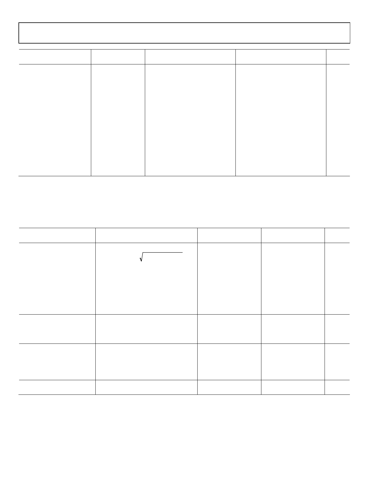
Parameter
DYNAMIC RESPONSE
Small Signal −3 dB
Bandwidth
G = +5
G = +100
G = +1000
Slew Rate
Settling Time to 0.01%
G = +5
G = +100
Settling Time to 0.01%
G = +5
G = +100
Overload Recovery
Conditions
Min
VS = ±5 V,
+5 V output step
VS = ±15 V,
+15 V output step
50% input overload
AD627A
Typ
Max
Min
80
3
0.4
+0.05/−0.06
135
350
330
330
560
560
3
3
1 Does not include effects of External Resistor RG.
2 See Table 8 for total RTI errors.
3 See the Using the AD627 section for more information on the input range, gain range, and common-mode range.
AD627B
Typ
Max
Unit
80
kHz
3
kHz
0.4
kHz
+0.05/−0.06
V/μs
135
μs
350
μs
μs
μs
μs
DUAL AND SINGLE SUPPLIES
Table 3.
Parameter
NOISE
Voltage Noise, 1 kHz
Input, Voltage Noise, eni
Output, Voltage Noise, eno
RTI, 0.1 Hz to 10 Hz
G = +5
G = +1000
Current Noise
0.1 Hz to 10 Hz
REFERENCE INPUT
RIN
Gain to Output
Voltage Range1
POWER SUPPLY
Operating Range
Quiescent Current
Over Temperature
TEMPERATURE RANGE
For Specified Performance
Conditions
Total RTI Noise = (eni )2 + (eno / RG )2
f = 1 kHz
RG = ∞
Dual supply
Single supply
AD627A
AD627B
Min Typ
Max Min Typ
Max Unit
38
177
1.2
0.56
50
1.0
125
1
±1.1
2.2
60
200
−40
38
177
1.2
0.56
50
1.0
125
1
±18 ±1.1
36 2.2
85
60
200
+85 −40
nV/√Hz
nV/√Hz
μV p-p
μV p-p
fA/√Hz
pA p-p
kΩ
±18 V
36 V
85 μA
nA/°C
+85 °C
1 See Using the AD627 section for more information on the reference terminal, input range, gain range, and common-mode range.
Rev. D | Page 6 of 24
Share Link: 