AD6672 查看數據表(PDF) - Analog Devices
零件编号
产品描述 (功能)
生产厂家
AD6672 Datasheet PDF : 30 Pages
| |||
AD6672
SWITCHING SPECIFICATIONS
Table 4.
Parameter
CLOCK INPUT PARAMETERS
Input Clock Rate
Conversion Rate1
CLK Period—Divide-by-1 Mode (tCLK)
CLK Pulse Width High (tCH)
Divide-by-1 Mode, DCS Enabled
Divide-by-1 Mode, DCS Disabled
Divide-by-2 Mode Through Divide-by-8 Mode
Aperture Delay (tA)
Aperture Uncertainty (Jitter, tJ)
DATA OUTPUT PARAMETERS
Data Propagation Delay (tPD)
DCO Propagation Delay (tDCO)
DCO-to-Data Skew (tSKEW)
Pipeline Delay (Latency)—NSR Disabled
Pipeline Delay (Latency)—NSR Enabled
Wake-Up Time (from Standby)
Wake-Up Time (from Power-Down)
Out-of-Range Recovery Time
1 Conversion rate is the clock rate after the divider.
Data Sheet
Temperature Min
Typ
Max
Unit
Full
Full
40
Full
4
625
MHz
250
MSPS
ns
Full
1.8
2.0
2.2
ns
Full
1.9
2.0
2.1
ns
Full
0.8
ns
Full
1.0
ns
Full
0.1
ps rms
Full
4.1
4.7
5.2
ns
Full
4.7
5.3
5.8
ns
Full
0.3
0.5
0.7
ns
Full
10
Cycles
Full
13
Cycles
Full
10
µs
Full
100
µs
Full
3
Cycles
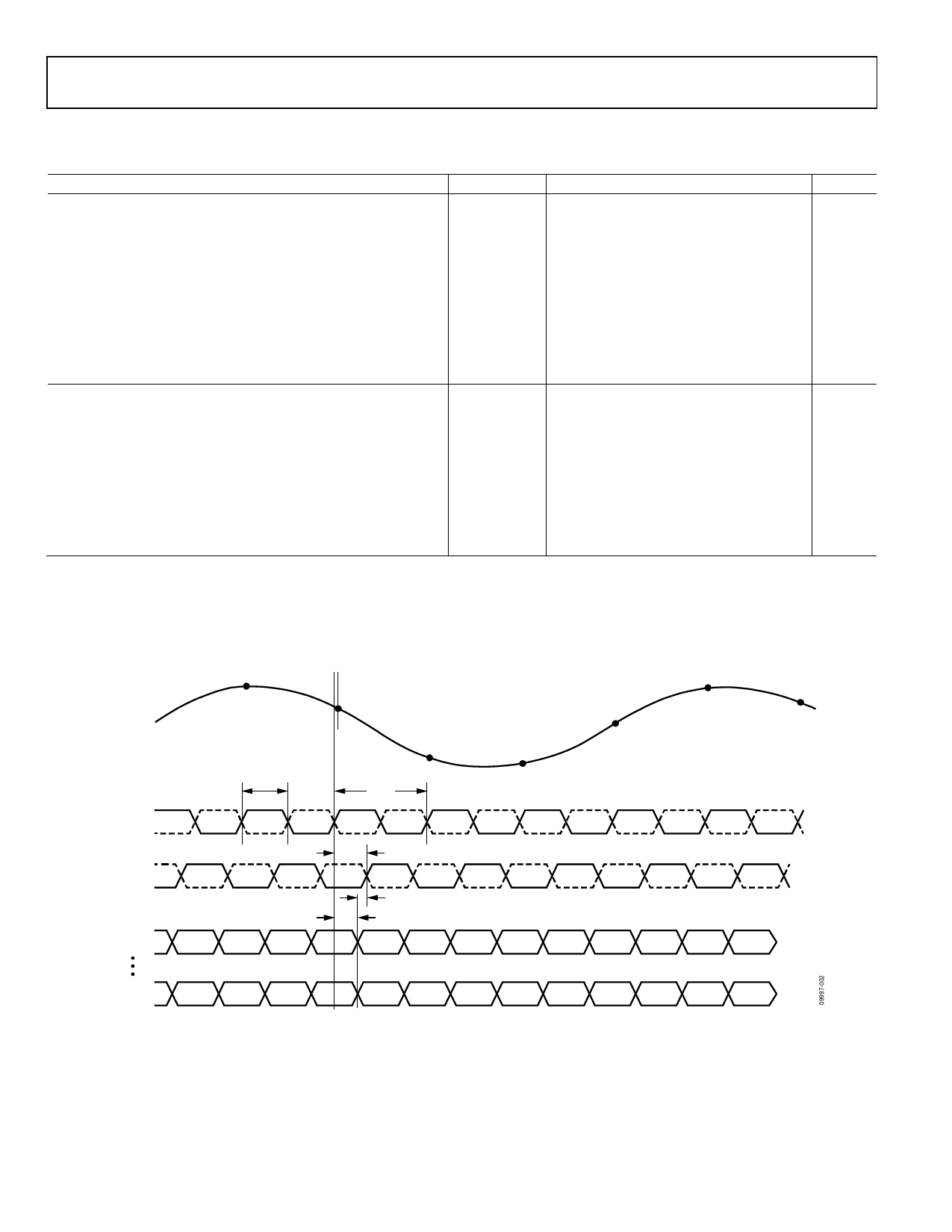
Timing Diagram
N–1
VIN
tCH
CLK+
CLK–
DCO–
DCO+
ODD/EVEN
0/D0±
(LSB)
D9±/D10±
(MSB)
tA
N
N+1
tCLK
N+2
N+3
N+4
N+5
tDCO
tSKEW
tPD
0
D0
N – 10 N – 10
0
N–9
D0
N–9
0
N–8
D0
N–8
0
N–7
D0
N–7
0
N–6
D9
D10
N – 10 N – 10
D9
N–9
D10
N–9
D9
N–8
Figure 2. LVDS Data Output Timing
D10
N–8
D9
N–7
D10
N–7
D9
N–6
Rev. C | Page 8 of 30
Share Link: 