AD7401YRWZ-REEL 查看數據表(PDF) - Analog Devices
零件编号
产品描述 (功能)
生产厂家
AD7401YRWZ-REEL Datasheet PDF : 20 Pages
| |||
AD7401
Parameter
POWER REQUIREMENTS
VDD1
VDD2
IDD1 6
IDD2 7
Y Version1, 2 Unit
4.5/5.25
3/5.5
12
8
4
V min/V max
V min/V max
mA max
mA max
mA max
Test Conditions/Comments
VDD1 = 5.25 V
VDD2 = 5.5 V
VDD2 = 3.3 V
1 Temperature range is −40°C to +85°C.
2 All voltages are relative to their respective ground.
3 See the Terminology section.
4 For fMCLK > 16 MHz to 20 MHz, mark space ratio is 48/52 to 52/48, VDD1 = VDD2 = 5 V ± 5% and TA = −40°C to +85°C.
5 Sample tested during initial release to ensure compliance.
6 See Figure 15.
7 See Figure 17.
TIMING SPECIFICATIONS1
VDD1 = 4.5 V to 5.25 V, VDD2 = 3 V to 5.5 V, TA = TMAX to TMIN, unless otherwise noted.
Table 2.
Parameter
fMCLKIN 2 , 3
t1 4
t24
t3
t4
Limit at TMIN, TMAX
20
5
25
15
0.4 × tMCLKIN
0.4 × tMCLKIN
Unit
MHz max
MHz min
ns max
ns min
ns min
ns min
Description
Master clock input frequency
Master clock input frequency
Data access time after MCLK rising edge
Data hold time after MCLK rising edge
Master clock low time
Master clock high time
1 Sample tested during initial release to ensure compliance.
2 Mark space ratio for clock input is 40/60 to 60/40 for fMCLKIN to 16 MHz and 48/52 to 52/48 for fMCLKIN > 16 MHz to 20 MHz.
3 VDD1 = VDD2 = 5 V ± 5% for fMCLKIN > 16 MHz to 20 MHz.
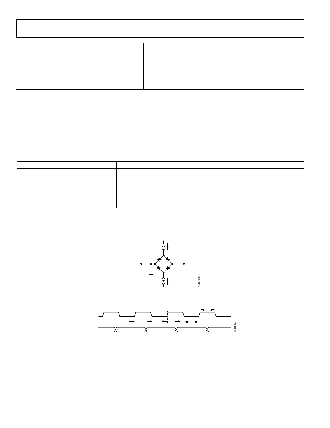
4 Measured with the load circuit of Figure 2 and defined as the time required for the output to cross 0.8 V or 2.0 V.
200µA
IOL
TO OUTPUT
PIN CL
25pF
1.6V
200µA
IOH
Figure 2. Load Circuit for Digital Output Timing Specifications
MCLKIN
MDAT
t4
t1
t2
t3
Figure 3. Data Timing
Rev. A | Page 4 of 20
Share Link: 