AD7414 وں¥çœ‹و•¸و“ڑè،¨ï¼ˆPDF) - Analog Devices
零ن»¶ç¼–هڈ·
ن؛§ه“پوڈڈè؟° (هٹں能)
ç”ںن؛§هژ‚ه®¶
AD7414 Datasheet PDF : 20 Pages
| |||
INTERNAL REGISTER STRUCTURE
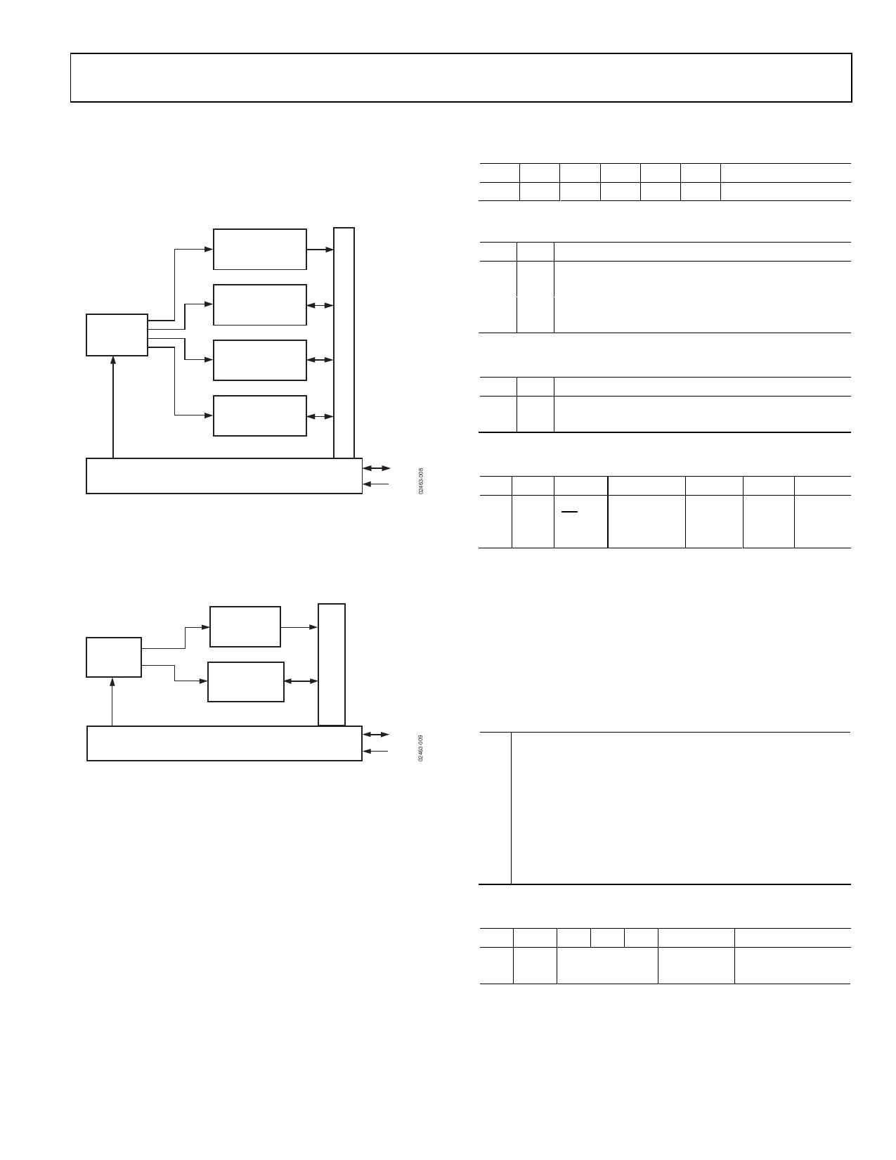
The AD7414 has five internal registers, as shown in Figure 8.
Four are data registers, and one is an address pointer register.
ADDRESS
POINTER
REGISTER
TEMPERATURE
VALUE
REGISTER
CONFIGURATION
REGISTER
D
A
T
THIGH
A
REGISTER
TLOW
REGISTER
SERIAL BUS INTERFACE
SDA
SCL
Figure 8. AD7414 Register Structure
The AD7415 has three internal registers, as shown in Figure 9.
Two are data registers, and one is an address pointer register.
ADDRESS
POINTER
REGISTER
TEMPERATURE
VALUE
REGISTER
D
A
T
CONFIGURATION
A
REGISTER
SDA
SCL
Figure 9. AD7415 Register Structure
Each data register has an address pointed to by the address
pointer register when communicating with it. The temperature
value register is the only data register that is read-only.
ADDRESS POINTER REGISTER
The address pointer register is an 8-bit register that stores an
address that points to one of the four data registers of the
AD7414 and one of the two data registers of the AD7415. The
first byte of every serial write operation to the AD7414/AD7415
is the address of one of the data registers, which is stored in the
address pointer register and selects the data register to which
subsequent data bytes are written. Only the 2 LSBs of this
register are used to select a data register.
AD7414/AD7415
Table 6. Address Pointer Register
P7 P6 P5 P4 P3 P2
000000
P1 P0
Register Select
Table 7. AD7414 Register Address
P1 P0 Register
0 0 Temperature value register (read-only)
0 1 Configuration register (read/write)
1 0 THIGH register (read/write)
1 1 TLOW register (read/write)
Table 8. AD7415 Register Address
P1 P0 Registers
0 0 Temperature value register (read-only)
0 1 Configuration register (read/write)
Table 9. AD7414 Configuration Register
D7 D6 D5
D4
D3
PD FLTR ALERT
EN
01 11
01
ALERT
POLARITY
01
ALERT
RESET
01
1 Default settings at power-up.
D2
ONE
SHOT
01
D1 D0
TEST
MODE
0s1
CONFIGURATION REGISTER (ADDRESS 0X01)
The configuration register is an 8-bit read/write register that is
used to set the operating modes of the AD7414/AD7415. In the
AD7414, six of the MSBs are used (D7 to D2) to set the
operating modes (see Table 10). D0 and D1 are used for factory
settings and must have zeros written to them during normal
operation.
Table 10. AD7414 Configuration Register Settings
D7 Full power-down if = 1.
D6 Bypass SDA and SCL filtering if = 0.
D5 Disable ALERT if = 1.
D4 ALERT is active low if D4 = 0, ALERT is active high if D4 = 1.
D3 Reset the ALERT pin if set to 1. The next temperature
conversion has the ability to activate the ALERT function.
The bit status is not stored; thus this bit is 0 if read.
D2 Initiate a one shot temperature conversion if set to a 1.
The bit status is not stored; thus this bit is 0 if read.
Table 11. AD7415 Configuration Register
D7 D6 D5 D4 D3 D2
D1 D0
PD FLTR TEST MODE ONE SHOT TEST MODE
01 11
0s1
0s1
0s1
1 Default settings at power-up.
Rev. E | Page 9 of 20
Share Link: 