AD7495BRM 查看數據表(PDF) - Analog Devices
零件编号
产品描述 (功能)
生产厂家
AD7495BRM Datasheet PDF : 24 Pages
| |||
AD7475/AD7495
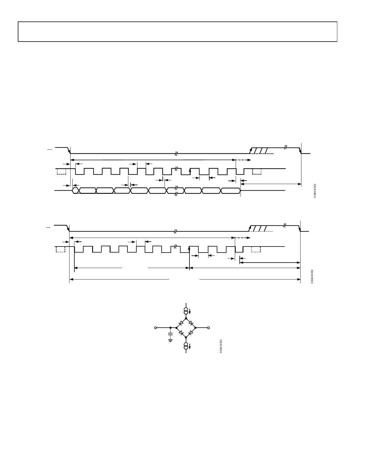
TIMING EXAMPLE 1
With fSCLK = 20 MHz and a throughput of 1 MSPS, the cycle
time is t2 + 12.5(1/fSCLK) + tACQ = 1 μs. With t2 = 10 ns min, tACQ
is 365 ns. The 365 ns satisfies the requirement of 300 ns for tACQ.
In Figure 3, tACQ comprises 2.5(1/fSCLK) + t8 + tQUIET, where t8 =
45 ns. This allows a value of 195 ns for tQUIET, satisfying the
minimum requirement of 100 ns.
TIMING EXAMPLE 2
With fSCLK = 5 MHz and a throughput of 315 KSPS, the cycle
time is t2 + 12.5(1/fSCLK) + tACQ = 3.174 μs. With t2 = 10 ns min,
tACQ is 664 ns. The 664 ns satisfies the requirement of 300 ns for
tACQ. In Figure 3, tACQ comprises 2.5(1/fSCLK) + t8 + tQUIET, where
t8 = 45 ns. This allows a value of 119 ns for tQUIET, satisfying the
minimum requirement of 100 ns. As in this example and with
other slower clock values, the signal may already be acquired
before the conversion is complete, but it is still necessary
to leave 100 ns minimum tQUIET between conversions. In
Example 2, the signal should be fully acquired at approximately
Point C in Figure 3.
CS
SCLK
t2
1
2
3
t3
SDATA
0
THREE-STATE
0
0
0
FOUR LEADING ZEROS
tCONVERT
t6
4
5
t4
DB11
t7
DB10
B
13
14
t5
15
16
t8
tQUIET
DB2
DB1
DB0
THREE-STATE
Figure 2. Serial Interface Timing Diagram
CS
SCLK
tCONVERT
t2
t6
B
C
1
2
3
4
5
13
14
15
16
10ns
12.5 (1/fSCLK)
t5
1/THROUGHPUT
t8
45ns
tACQUISITION
tQUIET
Figure 3. Serial Interface Timing Example
200μA
IOL
TO OUTPUT
PIN
CL
50pF
200μA
IOH
1.6V
Figure 4. Load Circuit for Digital Output Timing Specifications
Rev. B | Page 8 of 24
Share Link: 