AD7492BRUZ 查看數據表(PDF) - Analog Devices
零件编号
产品描述 (功能)
生产厂家
AD7492BRUZ Datasheet PDF : 24 Pages
| |||
AD7492
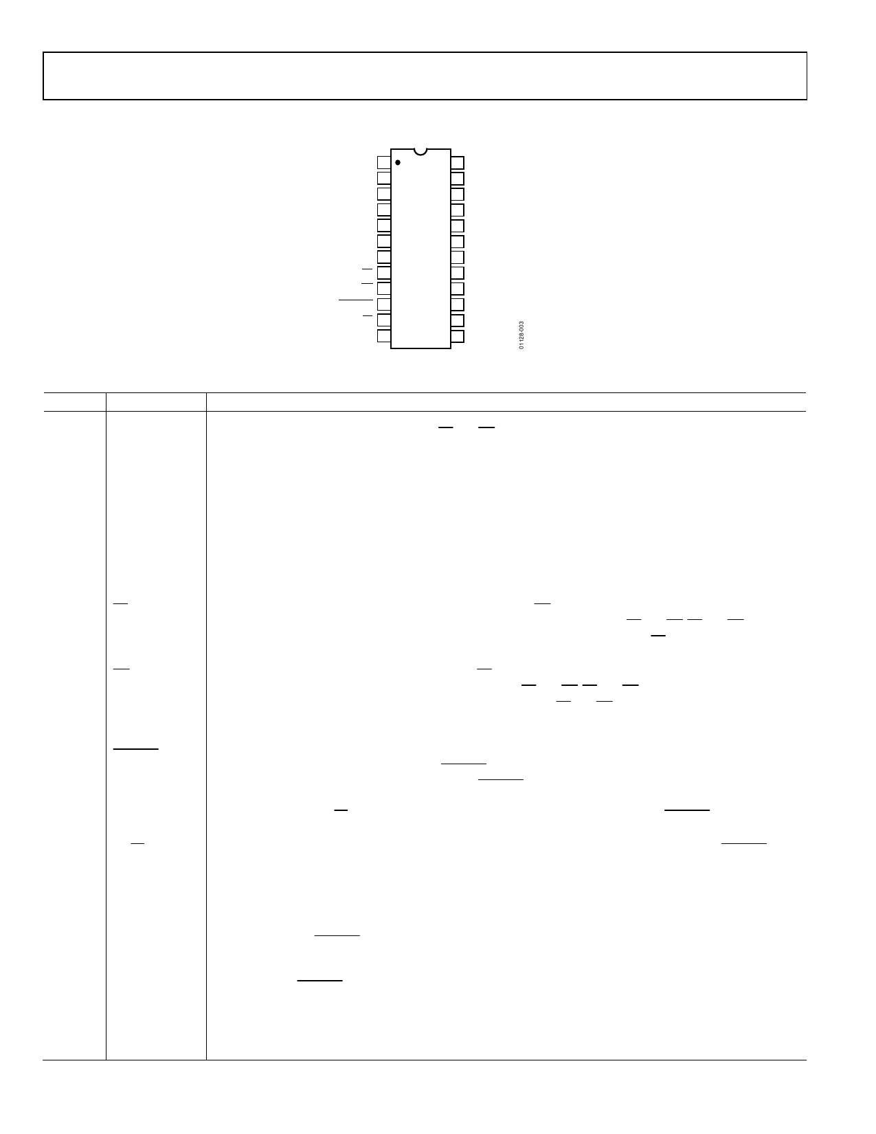
PIN CONFIGURATION AND FUNCTION DESCRIPTIONS
DB9 1
24 DB8
DB10 2
(MSB) DB11 3
23 DB7
22 DB6
AVDD 4
21 VDRIVE
REF OUT 5 AD7492 20 DVDD
VIN 6 TOP VIEW 19 DGND
AGND 7 (Not to Scale) 18 DB5
CS 8
17 DB4
RD 9
16 DB3
CONVST 10
PS/FS 11
BUSY 12
15 DB2
14 DB1
13 DB0 (LSB)
Figure 3. Pin Configuration
Table 5. Pin Function Descriptions
Pin
Mnemonic
Function
1 to 3, DB11 to DB0
13 to 18,
22 to 24
Data Bit 11 to Data Bit 0. Parallel digital outputs that provide the conversion result for the part. These are
three-state outputs that are controlled by CS and RD. The output high voltage level for these outputs is
determined by the VDRIVE input.
4
AVDD
Analog Supply Voltage, 2.7 V to 5.25 V. This is the only supply voltage for all analog circuitry on the AD7492.
The AVDD and DVDD voltages should ideally be at the same potential and must not be more than 0.3 V apart,
even on a transient basis. This supply should be decoupled to AGND.
5
REF OUT
Reference Out. The output voltage from this pin is 2.5 V ± 1%.
6
VIN
Analog Input. Single-ended analog input channel. The input range is 0 V to REFIN. The analog input presents
a high dc input impedance.
7
AGND
Analog Ground. Ground reference point for all analog circuitry on the AD7492. All analog input signals
should be referred to this AGND voltage. The AGND and DGND voltages should ideally be at the same
potential and must not be more than 0.3 V apart, even on a transient basis.
8
CS
Chip Select. Active low logic input used in conjunction with RD to access the conversion result. The
conversion result is placed on the data bus following the falling edge of both CS and RD. CS and RD are both
connected to the same AND gate on the input so the signals are interchangeable. CS can be hardwired
permanently low.
9
RD
Read Input. Logic input used in conjunction with CS to access the conversion result. The conversion result is
placed on the data bus following the falling edge of both CS and RD. CS and RD are both connected to the
same AND gate on the input so the signals are interchangeable. CS and RD can be hardwired permanently
low, in which case the data bus is always active and the result of the new conversion is clocked out slightly
before to the BUSY line going low.
10
CONVST
Conversion Start Input. Logic input used to initiate conversion. The input track/hold amplifier goes from track
mode to hold mode on the falling edge of CONVST and the conversion process is initiated at this point. The
conversion input can be as narrow as 10 ns. If the CONVST input is kept low for the duration of conversion
and is still low at the end of conversion, the part automatically enters a sleep mode. The type of sleep mode is
determined by the PS/FS pin. If the part enters a sleep mode, the next rising edge of CONVST wakes up the
part. Wake-up time depends on the type of sleep mode.
11
PS/FS
Partial Sleep/Full Sleep Mode. This pin determines the type of sleep mode the part enters if the CONVST pin is
kept low for the duration of the conversion and is still low at the end of conversion. In partial sleep mode the
internal reference circuit and oscillator circuit are not powered down and draws 250 μA maximum. In full
sleep mode all of the analog circuitry are powered down and the current drawn is negligible. This pin is
hardwired either high (DVDD) or low (GND).
12
BUSY
BUSY Output. Logic output indicating the status of the conversion process. The BUSY signal goes high after
the falling edge of CONVST and stays high for the duration of the conversion. Once the conversion is
complete and the conversion result is in the output register, the BUSY line returns low. The track/hold returns
to track mode just prior to the falling edge of BUSY and the acquisition time for the part begins when BUSY
goes low. If the CONVST input is still low when BUSY goes low, the part automatically enters its sleep mode
on the falling edge of BUSY.
19
DGND
Digital Ground. This is the ground reference point for all digital circuitry on the AD7492. The DGND and AGND
voltages should ideally be at the same potential and must not be more than 0.3 V apart, even on a transient
basis.
Rev. A | Page 8 of 24
Share Link: 