AD7520KN 查看數據表(PDF) - Intersil
零件编号
产品描述 (功能)
生产厂家
AD7520KN Datasheet PDF : 9 Pages
| |||
AD7520, AD7530, AD7521, AD7531
Pin Descriptions
AD7520/30 AD7521/31 PIN NAME
DESCRIPTION
1
1
IOUT1 Current Out summing junction of the R2R ladder network.
2
2
IOUT2 Current Out virtual ground, return path for the R2R ladder network.
3
3
GND Digital Ground. Ground potential for digital side of D/A.
4
4
Bits 1(MSB) Most Significant Digital Data Bit.
5
5
Bit 2
Digital Bit 2.
6
6
Bit 3
Digital Bit 3.
7
7
Bit 4
Digital Bit 4.
8
8
Bit 5
Digital Bit 5.
9
9
Bit 6
Digital Bit 6.
10
10
Bit 7
Digital Bit 7.
11
11
Bit 8
Digital Bit 8.
12
12
Bit 9
Digital Bit 9.
13
13
Bit 10 Digital Bit 10 (AD7521/31). Least Significant Digital Data Bit (AD7520/30).
-
14
Bit 11 Digital Bit 11 (AD7521/31).
-
15
Bit 12 Least Significant Digital Data Bit (AD7521/31).
14
16
V+
Power Supply +5V to +15V.
15
17
VREF Voltage Reference Input to set the output range. Supplies the R2R resistor ladder.
16
18
RFEEDBACK Feedback resistor used for the current to voltage conversion when using an external Op Amp.
Definition of Terms
Nonlinearity: Error contributed by deviation of the DAC
transfer function from a “best straight line” through the actual
plot of transfer function. Normally expressed as a percent-
age of full scale range or in (sub)multiples of 1 LSB.
Resolution: It is addressing the smallest distinct analog
output change that a D/A converter can produce. It is
commonly expressed as the number of converter bits. A
converter with resolution of n bits can resolve output changes
of 2-N of the full-scale range, e.g., 2-N VREF for a unipolar
conversion. Resolution by no means implies linearity.
Settling Time: Time required for the output of a DAC to set-
tle to within specified error band around its final value (e.g.,
1/2 LSB) for a given digital input change, i.e., all digital inputs
LOW to HIGH and HIGH to LOW.
Gain Error: The difference between actual and ideal analog
output values at full scale range, i.e., all digital inputs at
HIGH state. It is expressed as a percentage of full scale
range or in (sub)multiples of 1 LSB.
Feedthrough Error: Error caused by capacitive coupling
from VREF to IOUT1 with all digital inputs LOW.
Output Capacitance: Capacitance from IOUT1 and IOUT2
terminals to ground.
Output Leakage Current: Current which appears on IOUT1
terminal when all digital inputs are LOW or on IOUT2
terminal when all digital inputs are HIGH.
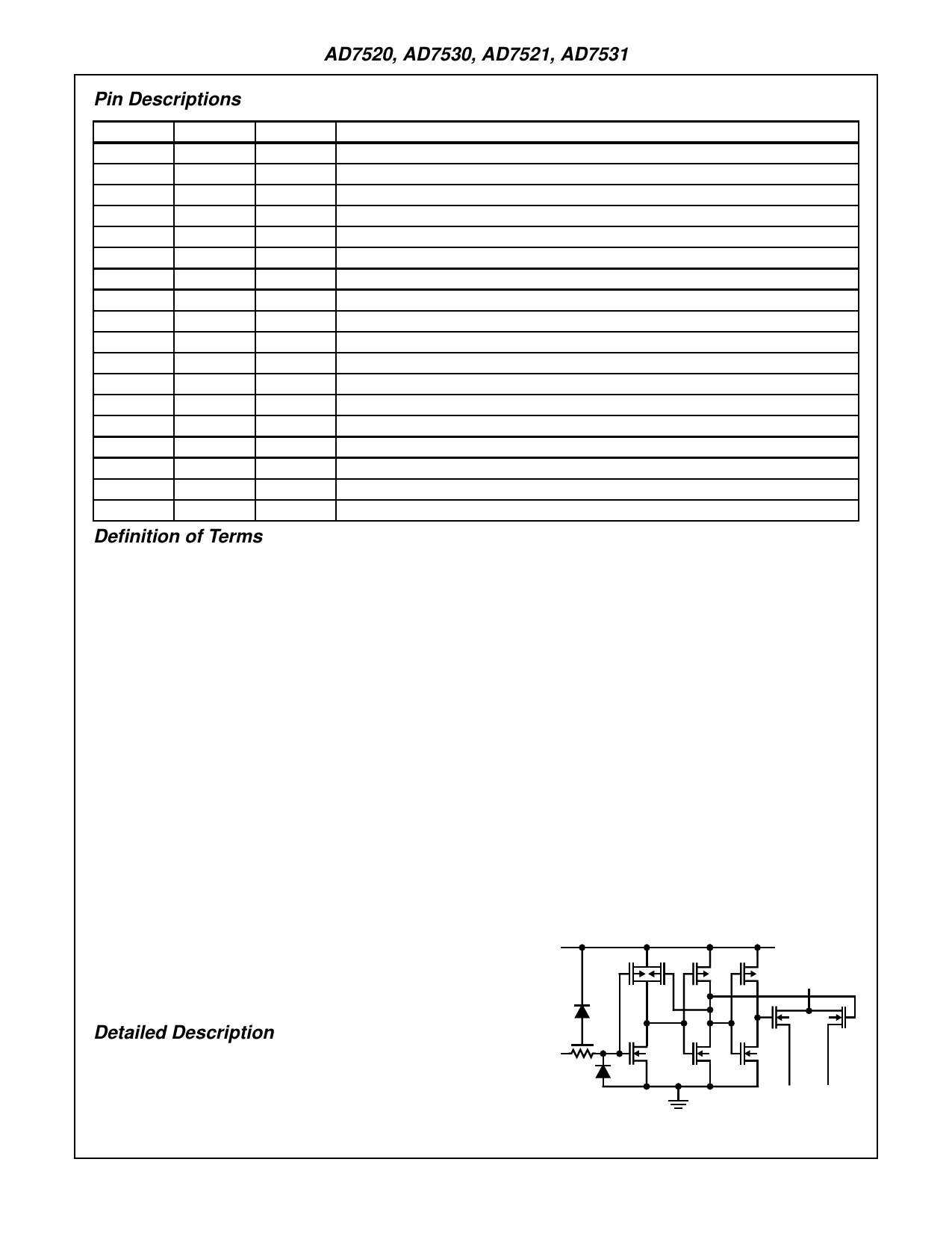
Detailed Description
The AD7520, AD7530, AD7521 and AD7531 are monolithic,
multiplying D/A converters. A highly stable thin film R-2R
resistor ladder network and NMOS SPDT switches form the
basis of the converter circuit, CMOS level shifters permit low
power TTL/CMOS compatible operation. An external voltage
or current reference and an operational amplifier are all that
is required for most voltage output applications.
A simplified equivalent circuit of the DAC is shown in the
Functional Diagram. The NMOS SPDT switches steer the lad-
der leg currents between IOUT1 and IOUT2 buses which must
be held either at ground potential. This configuration main-
tains a constant current in each ladder leg independent of the
input code.
Converter errors are further reduced by using separate
metal interconnections between the major bits and the
outputs. Use of high threshold switches reduce offset (leak-
age) errors to a negligible level.
The level shifter circuits are comprised of three inverters with
positive feedback from the output of the second to the first, see
Figure 1. This configuration results in TTL/CMOS compatible
operation over the full military temperature range. With the lad-
der SPDT switches driven by the level shifter, each switch is
binarily weighted for an ON resistance proportional to the
respective ladder leg current. This assures a constant voltage
drop across each switch, creating equipotential terminations for
the 2R ladder resistors and highly accurate leg currents.
V+
13
4
6 TO LADDER
DTL/TTL/
CMOS INPUT
89
2
5
7
FIGURE 1. CMOS SWITCH
IOUT2 IOUT1
10-10
Share Link: 