AD7538 查看數據表(PDF) - Analog Devices
零件编号
产品描述 (功能)
生产厂家
AD7538 Datasheet PDF : 16 Pages
| |||
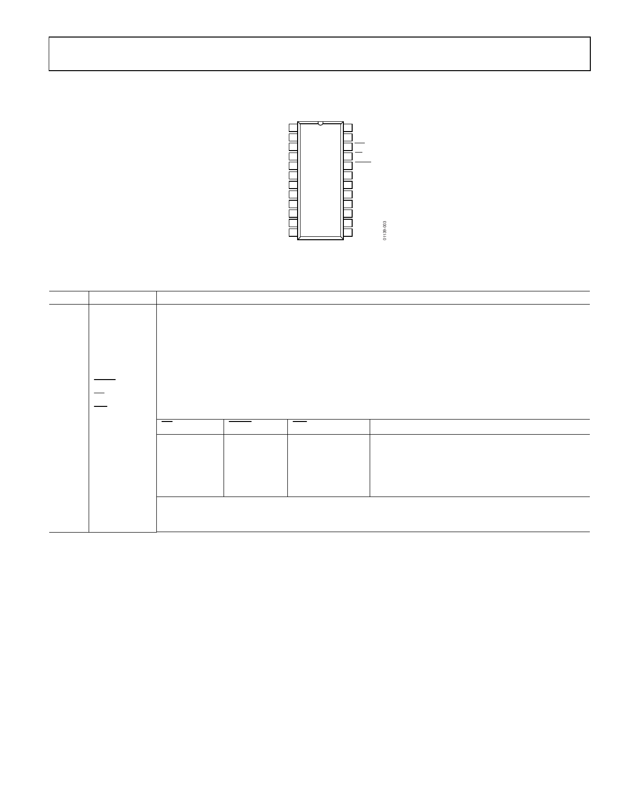
PIN CONFIGURATION AND FUNCTION DESCRIPTIONS
AD7538
VREF 1
24 VSS
RFB 2
23 VDD
IOUT 3
22 WR
AGND 4
DGND 5
21 CS
AD7538
TOP VIEW
20 LDAC
(MSB) DB13 6 (Not to Scale) 19 DB0 (LSB)
DB12 7
18 DB1
DB11 8
17 DB2
DB10 9
16 DB3
DB9 10
15 DB4
DB8 11
14 DB5
DB7 12
13 DB6
Figure 3. Pin Configuration
Table 5. Pin Function Description
Pin No. Mnemonic
Description
1
VREF
2
RFB
3
IOUT
4
AGND
Voltage Reference.
Feedback Resistor. Used to close the loop around an external op amp.
Current Output Terminal.
Analog Ground
5
DGND
Digital Ground.
6 to 19 DB13 to DB0 Data Inputs. Bit DB13 (MSB) to Bit DB0 (LSB).
20
LDAC
Chip Select Input. Active low.
21
CS
Asynchronous Load DAC Input. Active low.
22
WR
Write Input. Active low.
CS
LDAC
WR
Operation
0
1
0
1
0
X1
Load input register.
Load DAC register from input register.
23
VDD
24
VSS
0
0
0
Input and DAC registers are transparent.
1
1
X1
No operation.
X1
1
1
X
No operation.
+12 V to +15 V Supply Input.
Bias pin for high temperature low leakage configuration. To implement low leakage system, the pin should be
at a negative voltage. See Figure 6 and Figure 8 for recommended circuitry.
1 X = don’t care.
Rev. B | Page 7 of 16
Share Link: 