AD7801 查看數據表(PDF) - Analog Devices
零件编号
产品描述 (功能)
生产厂家
AD7801 Datasheet PDF : 16 Pages
| |||
AD7801
In the circuit shown the LDAC is hardwired low thus the DAC
output is updated on the rising edge of WR. Some applications
may require synchronous updating of the DAC in the AD7801.
In this case the LDAC signal can be driven from an external
timer or can be controlled by the microprocessor. One option
for synchronous updating is to decode the LDAC from the ad-
dress bus so a write operation at this address will synchronously
update the DAC output. A simple OR gate with one input
driven from the decoded address and the second input from the
WR signal will implement this function.
AD7801–8051/8088 Interface
Figure 31 shows a serial interface between the AD7801 and the
8051/8088 processors.
A15
ADDRESS BUS
A8
PSEN OR DEN
WR
8051/8088*
ALE
EN ADDR
DECODE
OCTAL
LATCH
AD7801*
CS
WR
LDAC
DB7
DB0
AD7
AD0
DATA BUS
*ADDITIONAL CIRCUITRY OMITTED FOR CLARITY.
Figure 31. AD7801–8051/8088 Interface
APPLICATIONS
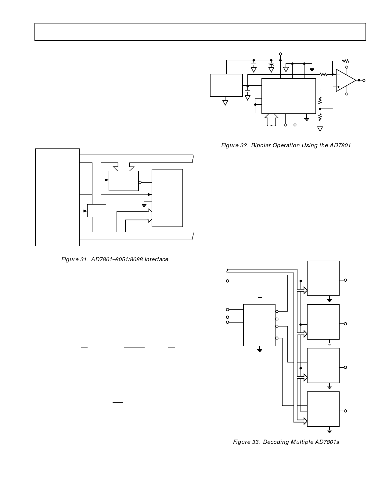
Bipolar Operation Using the AD7801
The AD7801 has been designed for unipolar operation but
bipolar operation is possible using the circuit in Figure 32. The
circuit shown is configured for an output voltage range of –5 V
to +5 V. Rail-to-rail operation at the amplifier output is achievable
by using an AD820 or OP295 as the output amplifier.
The output voltage for any input code can be calculated as
follows:
( ) VO
=
R2
1+
R4
R3
/
R1+ R2
×
2V REF
256
D
−V
REF
R4
R3
Where D is the decimal equivalent of the code loaded to the
DAC and VREF is the reference voltage input.
With VREF = 2.5 V, R1 = R3 = 10 kΩ and R2 = R4 = 20 kΩ and
VDD = 5 V.
VO
=
10D
256
–5
VDD = 3V TO 5V
0.1F 10F
R3
10kΩ
VIN
EXT REF VOUT
GND
AD780/REF192
WITH VDD = 5V
OR
AD589 WITH VDD = 3V
VDD AGND DGND
REF IN
0.1F
VOUT
AD7801
CLR
PD
D7-D0 CS WR LDAC
VDD
R1
10kΩ
R2
20kΩ
DATA CONTROL
BUS INPUTS
R4
20kΩ
+5V
AD820/
OP295
±5V
–5V
Figure 32. Bipolar Operation Using the AD7801
Decoding Multiple AD7801s in a System
The CS pin on the AD7801 can be used in applications to
decode a number of DACs. In this application, all DACs in the
system receive the same input data, but only the CS to one of
the DACs will be active at any one time allowing access to one
channel in the system. The 74HC139 is used as a two-to-four
line decoder to address any of the DACs in the system. To
prevent timing errors from occurring, the Enable input on the
74HC139 should be brought to its inactive state while the
Coded Address inputs are changing state. Figure 33 shows a
diagram of a typical setup for decoding multiple AD7801
devices in a system. The built-in power-on reset circuit on the
AD7801 ensures that the outputs of all DACs in the system
power up with zero volts on their outputs.
DATA BUS
WR
VDD
ENABLE
CODED
ADDRESS
1G
VCC
1Y0
1A
1Y1
1B
1Y2
74HC139
1Y3
DGND
AD7801
CS
WR
D0
D7
LDAC
VOUT
AD7801
CS
WR
D0
D7
LDAC
VOUT
AD7801
CS
WR
D0
D7
LDAC
VOUT
AD7801
CS
WR
D0
D7
LDAC
VOUT
Figure 33. Decoding Multiple AD7801s
REV. 0
–11–
Share Link: 