AD7818ARMZ 查看數據表(PDF) - Analog Devices
零件编号
产品描述 (功能)
生产厂家
AD7818ARMZ Datasheet PDF : 20 Pages
| |||
Data Sheet
DC Acquisition Time
The ADC starts a new acquisition phase at the end of a conversion
and ends on the falling edge of the CONVST signal. At the end
of a conversion, a settling time is associated with the sampling
circuit. This settling time lasts approximately 100 ns. The
analog signal on VIN is also being acquired during this settling
time. Therefore, the minimum acquisition time needed is
approximately 100 ns.
Figure 10 shows the equivalent charging circuit for the sampling
capacitor when the ADC is in its acquisition phase. R2 represents
the source impedance of a buffer amplifier or resistive network,
R1 is an internal multiplexer resistance, and C1 is the sampling
capacitor.
R2
VIN
R1
1kΩ
C1
3pF
Figure 10. Equivalent Sampling Circuit
During the acquisition phase, the sampling capacitor must be
charged to within a 1/2 LSB of its final value. The time it takes
to charge the sampling capacitor (TCHARGE) is given by
TCHARGE = 7.6 × (R2 + 1 kΩ) × 3 pF
For small values of source impedance, the settling time associated
with the sampling circuit (100 ns) is, in effect, the acquisition
time of the ADC. For example, with a source impedance (R2) of
10 Ω, the charge time for the sampling capacitor is approximately
23 ns. The charge time becomes significant for source impedances
of 1 kΩ and greater.
AC Acquisition Time
In ac applications, it is recommended to always buffer analog
input signals. The source impedance of the drive circuitry must
be kept as low as possible to minimize the acquisition time of
the ADC. Large values of source impedance cause the THD to
degrade at high throughput rates.
AD7817/AD7818
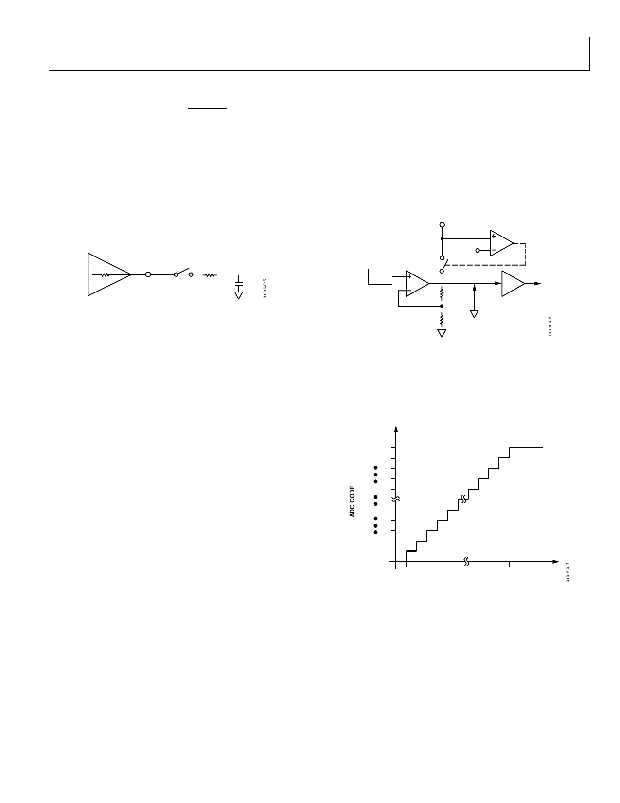
ON-CHIP REFERENCE
The AD7817/AD7818 have an on-chip, 1.2 V band gap reference
that is gained up to give an output of 2.5 V. By connecting the
REFIN pin to analog ground, the on-chip reference is selected.
This selection causes SW1 to open and the reference amplifier
to power up during a conversion (see Figure 11). Therefore, the
on-chip reference is not available externally. An external 2.5 V
reference can be connected to the REFIN pin, which has the
effect of shutting down the on-chip reference circuitry and
reducing IDD by approximately 0.25 mA.
REFIN
EXTERNAL
REFERENCE
DETECT
1.2V
SW1
1.2V
26kΩ
2.5V
BUFFER
24kΩ
Figure 11. On-Chip Reference
ADC TRANSFER FUNCTION
The output coding of the AD7817/AD7818 is straight binary. The
designed code transitions occur at successive integer LSB values
(that is, 1 LSB, 2 LSBs, and so on). The LSB size is = 2.5 V/1024 =
2.44 mV. The ideal transfer characteristic is shown in Figure 12.
111...111
111...110
111...000
011...111
1LSB = 2.5/1024
2.44mV
000...010
000...001
000...000
0V
1LSB
ANALOG INPUT
+2.5V × 1LSB
Figure 12. ADC Transfer Function
Rev. D | Page 13 of 20
Share Link: 