AD8067 查看數據表(PDF) - Analog Devices
零件编号
产品描述 (功能)
生产厂家
AD8067 Datasheet PDF : 24 Pages
| |||
AD8067
ABSOLUTE MAXIMUM RATINGS
Table 4.
Parameter
Supply Voltage
Power Dissipation
Common-Mode Input Voltage
Differential Input Voltage
Storage Temperature Range
Operating Temperature Range
Lead Temperature (Soldering 10 sec)
Junction Temperature
Rating
26.4 V
See Figure 3
VEE – 0.5 V to VCC + 0.5 V
1.8 V
–65°C to +125°C
–40°C to +85°C
300°C
150°C
Stresses above those listed under Absolute Maximum Ratings
may cause permanent damage to the device. This is a stress
rating only; functional operation of the device at these or any
other conditions above those indicated in the operational
section of this specification is not implied. Exposure to absolute
maximum rating conditions for extended periods may affect
device reliability.
MAXIMUM POWER DISSIPATION
The associated raise in junction temperature (TJ) on the die
limits the maximum safe power dissipation in the AD8067
package. At approximately 150°C, which is the glass transition
temperature, the plastic changes its properties. Even temporarily
exceeding this temperature limit can change the stresses that the
package exerts on the die, permanently shifting the parametric
performance of the AD8067. Exceeding a junction temperature
of 175°C for an extended period can result in changes in the
silicon devices, potentially causing failure.
The power dissipated in the package (PD) is the sum of the
quiescent power dissipation and the power dissipated in the
package due to the load drive. The quiescent power is the
voltage between the supply pins (VS) times the quiescent
current (IS). Assuming the load (RL) is referenced to midsupply,
the total drive power is VS/2 × IOUT, some of which is dissipated
in the package and some in the load (VOUT × IOUT). The
difference between the total drive power and the load power is
the drive power dissipated in the package. RMS output voltages
should be considered.
Data Sheet
PD = Quiescent Power + (Total Drive Power − Load Power)
( ) PD =
VS × IS
+
VS
2
× VOUT
RL
–
VOUT
RL
2
If RL is referenced to VS− as in single-supply operation, then the
total drive power is VS × IOUT.
If the rms signal levels are indeterminate, then consider the
worst case, when VOUT = VS/4 for RL to midsupply:
PD
= (VS
×IS )
+
(VS/4)2
RL
In single-supply operation with RL referenced to VS−, worst case
is VOUT = VS/2.
Airflow increases heat dissipation effectively, reducing θJA. In
addition, more metal directly in contact with the package leads
from metal traces, through holes, ground, and power planes
reduces the θJA.
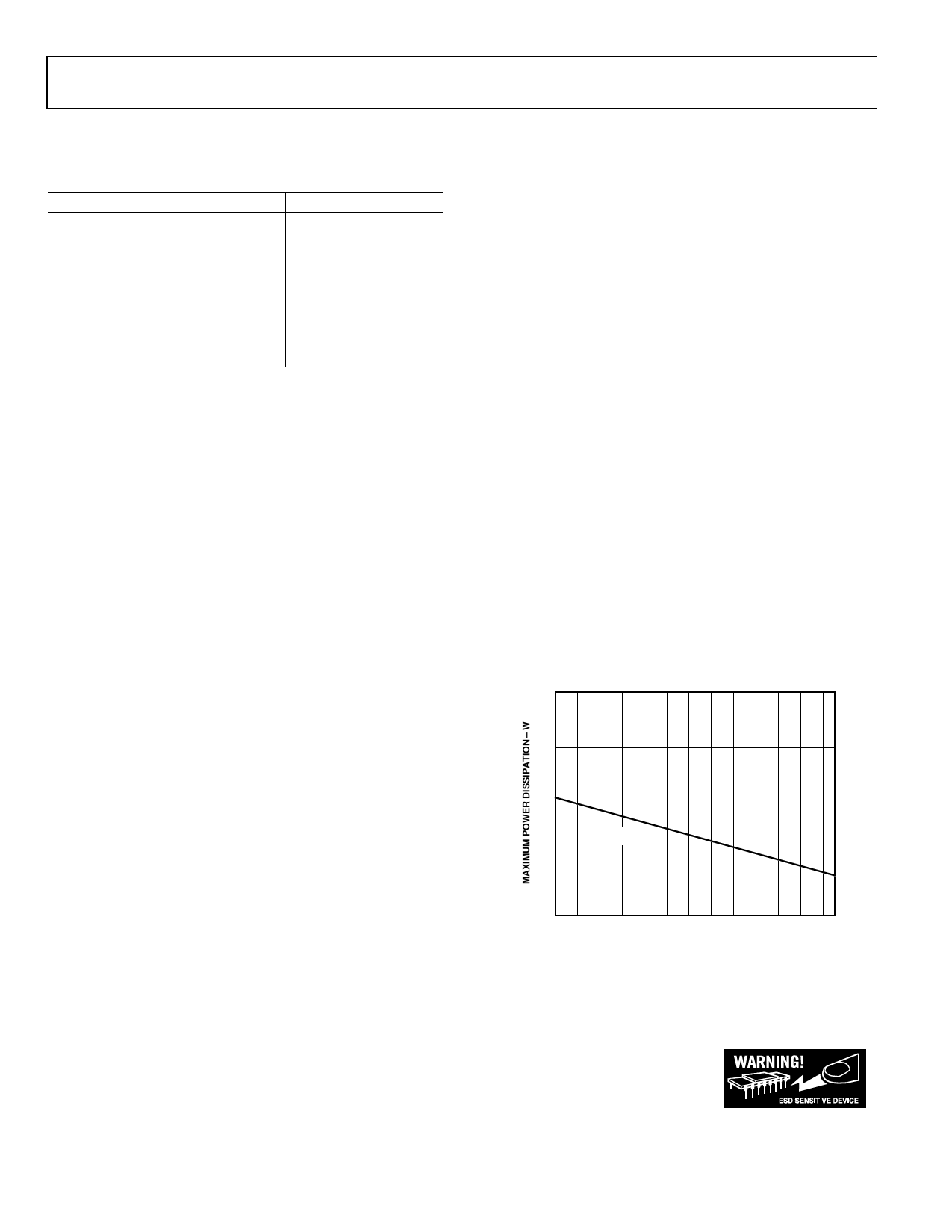
Figure 3 shows the maximum safe power dissipation in the
package vs. the ambient temperature for the SOT-23-5
(180°C/W) package on a JEDEC standard 4-layer board. θJA
values are approximations.
It should be noted that for every 10°C rise in temperature, IB
approximately doubles (see Figure 22).
2.0
1.5
1.0
SOT-23-5
0.5
0
–40 –30 –20 –10 0 10 20 30 40 50 60 70 80
AMBIENT TEMPERATURE – °C
Figure 3. Maximum Power Dissipation vs. Temperature for a 4-Layer Board
ESD CAUTION
ESD (electrostatic discharge) sensitive device. Electrostatic charges as high as 4000 V readily accumulate on
the human body and test equipment and can discharge without detection. Although this product features
proprietary ESD protection circuitry, permanent damage may occur on devices subjected to high energy
electrostatic discharges. Therefore, proper ESD precautions are recommended to avoid performance
degradation or loss of functionality.
Rev. B | Page 6 of 24
Share Link: 