AD8235 查看數據表(PDF) - Analog Devices
零件编号
产品描述 (功能)
生产厂家
AD8235 Datasheet PDF : 20 Pages
| |||
AD8235
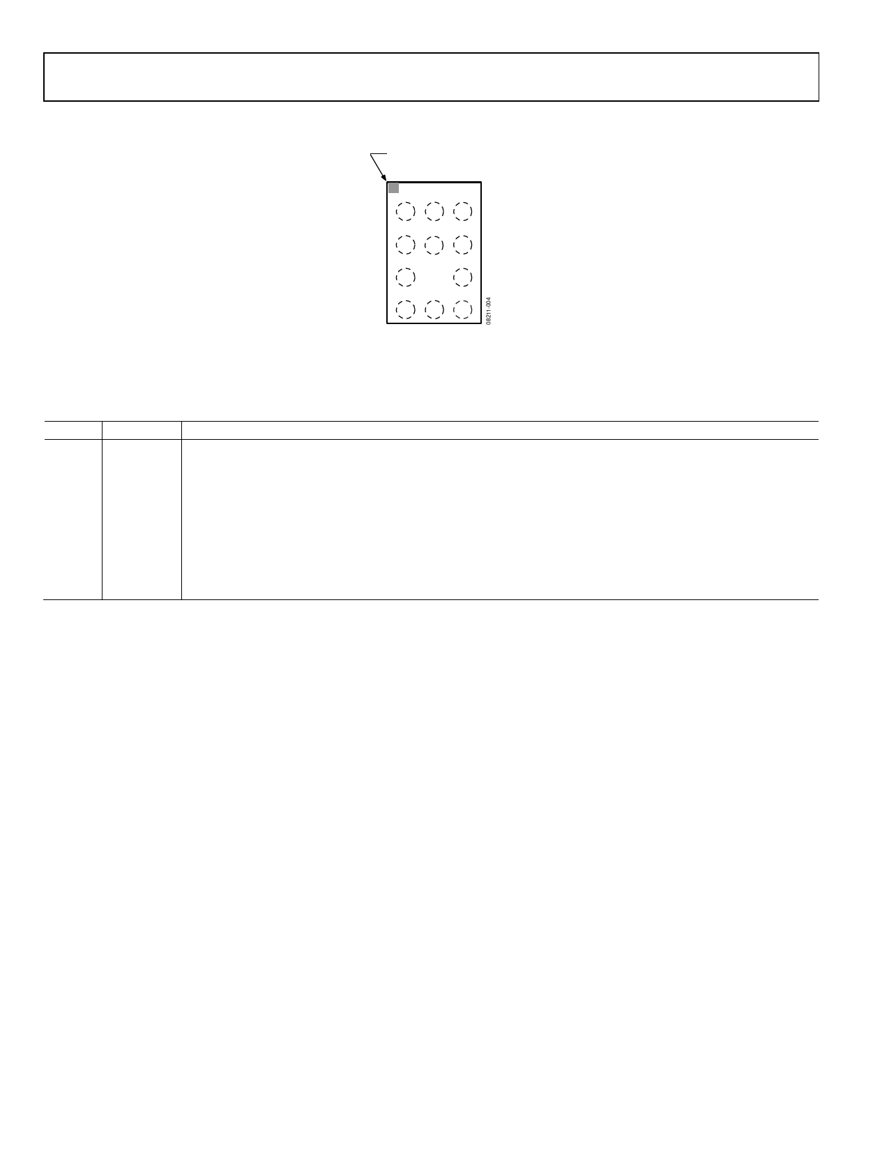
PIN CONFIGURATION AND FUNCTION DESCRIPTIONS
BALL A1
INDICATOR
1
2
3
+VS SDN –IN
A
VOUT NC RG
B
REF
RG
C
–VS NC +IN
D
TOP VIEW
(BALL SIDE DOWN)
Not to Scale
NC = NO CONNECT
Figure 4. Pin Configuration (Top View Looking Through Package)
Table 5. Pin Function Descriptions
Pin No. Mnemonic Description
A1
+VS
Positive Power Supply Terminal.
B1
VOUT
Output Terminal.
C1
REF
Reference Voltage Terminal. Drive this terminal with a low impedance voltage source to level-shift the output.
D1
−VS
Negative Power Supply Terminal.
A2
SDN
Shutdown Pin. Tie to −VS for shutdown. Tie to +VS for normal operation.
B2, D2 NC
No Connect. Leave both pins floating. Should not connect to any potential.
A3
−IN
Negative Input Terminal (True Differential Input).
B3, C3 RG
Gain Setting Terminals. Place resistor across the RG pins.
D3
+IN
Positive Input Terminal (True Differential Input).
Rev. 0 | Page 8 of 20
Share Link: 