ICS9178-03 жҹҘзңӢж•ёж“ҡиЎЁпјҲPDFпјү - Integrated Circuit Systems
йӣ¶д»¶зј–еҸ·
дә§е“ҒжҸҸиҝ° (еҠҹиғҪ)
з”ҹдә§еҺӮ家
ICS9178-03 Datasheet PDF : 8 Pages
| |||
ICS9178-03
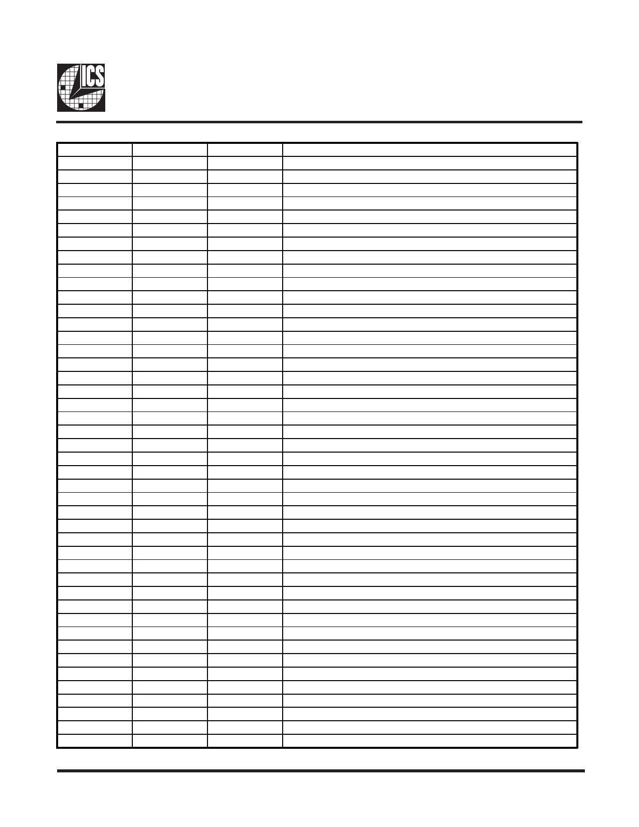
Pin Description
PIN NUMBER
32
31
6
5
30
29
3
2
1
4
44
43
42
41
28
27
11
10
8
7
22
21
24
23
20
38*
37*
36
35
25
26
19
16
17
15
14
13
12
18
40
39
9
33
34
PIN NAME
XAS0
XAS1
XCLKA0
XCLKA1
XBS0
XBS1
XCLKB0
XCLKB1
VDDXBA
GNDXBA
GNDXC
XCLKC0
XCLKC1
VDDXC
XCS0
XCS1
PCLK0
PCLK1
GNDP
VDDP
2XPCLK0
2XPCLK1
EVDD
EGND
EGND
FS0
FS1
FBCLK
REFCLK
AVDD
AGND
DCLK
VDDD
GNDD
BCLK0
BCLK1
GNDBAB
VDDBAB
ABCLK
TCLK
TEN#
RESET#
VDD
GND
TYPE
Input
Input
Output
Output
Input
Input
Output
Output
вҖ”
вҖ”
вҖ”
Output
Output
вҖ”
Input
Input
Output
Output
вҖ”
вҖ”
Output
Output
вҖ”
вҖ”
вҖ”
Input
Input
Input
Input
вҖ”
вҖ”
Output
вҖ”
вҖ”
Output
Output
вҖ”
вҖ”
Output
Input
Input
Input
вҖ”
вҖ”
DESCRIPTION
LSB Programmable Group A frequency selector.
MSB Programmable Group A frequency selector.
TTL/CMOS group A programmable clock output.
TTL/CMOS group A programmable clock output.
LSB Programmable Group B frequency selector.
MSB Programmable Group B frequency selector.
TTL/CMOS Group B programmable clock output.
TTL/CMOS Group B programmable clock output.
Power for programmable Group A and B buffers (Pins 2, 3, 5, 6).
Ground for programmable Group A and B buffers (Pins 2, 3, 5, 6).
Ground for the programmable Group C buffers (Pins 42 and 43).
TTL/CMOS Group C programmable clock output.
TTL/CMOS Group C programmable clock output.
Power for the XC signal output buffers (Pins 42 and 43).
LSB Programmable Group C frequency selector.
MSB Programmable Group C frequency selector.
TTL/CMOS 1X Processor clock output.
TTL/CMOS 1X Processor clock output.
Ground for PCLK output buffers (Pins 11 and 10).
Power for PCLK output buffers (Pins 11 and 10).
PECL 2X Processor clock output.
PECL 2X Processor clock output.
Power for PECL buffers (Pins 21 and 22).
Ground for PECL buffers (Pins 21 and 22).
Ground for PECL buffers (Pins 21 and 22).
LSB frequency select PLL (divider mode control).
MSB frequency select PLL (divider mode control).
External PLL feedback path from one of the BCLK outputs.
External reference clock input.
Power for the analog PLL circuitry.
Ground for the analog PLL circuitry.
TTL/CMOS D clock output.
Power for D output buffers (Pin 19).
Ground for D output buffer (Pin 19).
TTL/CMOS B (Bus) clock output.
TTL/CMOS B (Bus) clock output.
Ground for output buffers AB and B clocks (Pins 14, 15 & 18).
Power for output buffers AB and B clocks (Pins 14, 15 & 18).
TTL/CMOS AB Bus clock (has Asymmetric duty cycle).
External test clock input.
Test enable (tie low).
Sync register reset (active low).
Digital power supply for 5.0 or 3.3V.
Digital ground supply.
*=Pin is pulled-up to VDD internally by the device.
3
Share Link: 