AD846 查看數據表(PDF) - Analog Devices
零件编号
产品描述 (功能)
生产厂家
AD846 Datasheet PDF : 12 Pages
| |||
AD846
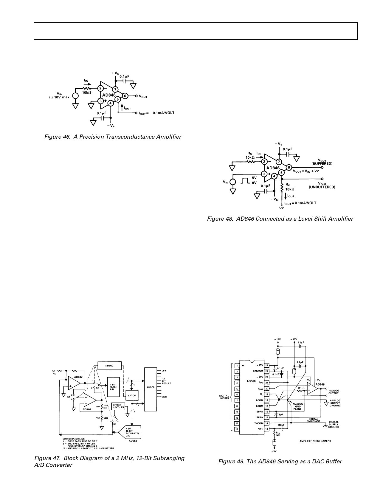
This compensation node may also be used as an additional
output terminal as in the precision transconductance amplifier
application of Figure 46.
Figure 46. A Precision Transconductance Amplifier
The AD846 can be used in either the inverting transconduc-
tance mode as shown in Figure 46, or in a noninverting mode
with RS grounded and VIN applied to the noninverting terminal.
The current output is essentially constant over a compliance
range of ± 10 V at the compensation node. The output current
(from Pin 5) is limited to about ± 1 mA due to internal satura-
tion. Under these circumstances the normal output pin provides
a buffered version of the compensation node output voltage.
Output load impedance of 500 Ω or greater will not affect the
accuracy of the transconductance conversion.
THE AD846 IN A 2 MHz, 12-BIT SUBRANGING A/D
CONVERTER CIRCUIT
The combination of fast settling times at high gains and low
dc errors make the AD846 ideal for use as an error amplifier in
high speed, 12-bit subranging A-D applications. In the circuit
of Figure 47, an AD842 serves as an input amplifier. First pass
conversion is accomplished, in a straightforward manner,
determining the top 7 bits. The latch then holds these top 7 bits
which are applied to a 7 bit, 12-bit accurate DAC and also to
the highest 7 bits of the adder (note that a sample-and-hold
should be used ahead of this converter to minimize errors due
to its 500 ns acquisition time). In the second pass, the input
switches S1 and S2 and S3 are set to state 2. The DAC output
is then subtracted from the input signal and the resulting
difference is then amplified by an AD846 gain of 32 follower.
This gain, together with a 1/64th scale offset, insures a unipolar
residue which can be converted by the flash A-D. Conversion is
accomplished via switches S1, S2 and S3 in state 1. Switch S1
connects the input signal of the AD846 residue amplifier to
ground which minimized overload recovery time.
THE AD846 AS AN OPEN-LOOP LEVEL SHIFTER
The AD846 can also be used for open-loop level shifting. As
shown in Figure 48, resistor RS is used to develop an input cur-
rent which is proportional to the input voltage, VIN. This current
flows from the compensation node (Pin 5) developing a voltage
across resistor RC (RC is equal in value to resistor RS) which,
rather than being grounded, has one end tied to reference volt-
age V2. The voltage appearing at Pin 5 is, therefore, voltage VIN
plus voltage V2 and will directly follow changes in VIN. By scal-
ing resistor RC, a level shift with voltage gain can be produced.
In addition, the normal voltage output at Pin 6 is approximately
equal to the voltage at Pin 5 thus providing a low impedance,
buffered output for the level shifter.
Figure 48. AD846 Connected as a Level Shift Amplifier
THE AD846 AS A HIGH SPEED DAC BUFFER
The AD846 will enable the AD568 12-bit DAC to develop
a 10 V output step which settles to within 0.025 percent of
itsfinal value in about 100 ns. This AD846/AD568 combina-
tion is shown in the circuit of Figure 49. Correct power
supply decoupling is essential: a 2.2 µF tantalum capacitor con-
nected in parallel with a 0.1 µF to 0.01 µF ceramic disc capacitor
is usually sufficient. These should be placed as close to the power
supply pins as possible. Also, a ground plane should be employed;
this ensure that there is a low impedance signal path to ground
which allows the fastest possible output settling. In 12-bit
systems with the AD846 operating at gains of 10 or less, inad-
equate supply decoupling can cause the output settling to
degrade from 100 ns to as much as 300 ns, with a 10 V output
step applied.
Figure 47. Block Diagram of a 2 MHz, 12-Bit Subranging
A/D Converter
REV. C
–11–
Figure 49. The AD846 Serving as a DAC Buffer
Share Link: 