AD9874 查看數據表(PDF) - Analog Devices
零件编号
产品描述 (功能)
生产厂家
AD9874 Datasheet PDF : 40 Pages
| |||
AD9874
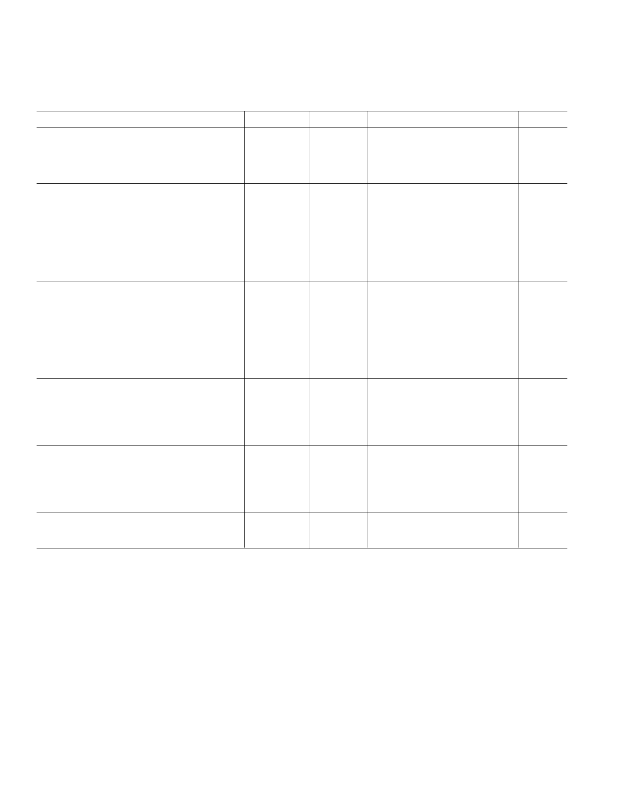
DIGITAL SPECIFICATIONS (VDDI = VDDF = VDDA = VDDC = VDDL = VDDD = VDDH = 2.7 V to 3.6 V, VDDQ = VDDP = 2.7 V to 5.5 V,
fCLK = 18 MSPS, fIF = 109.65 MHz, fLO = 107.4 MHz, fREF = 16.8 MHz, unless otherwise noted.)1
Parameter
Temp
Test Level Min
Typ
Max Unit
DECIMATOR
Decimation Factor2
Pass-Band Width
Pass-Band Gain Variation
Alias Attenuation
Full
IV
Full
V
Full
IV
Full
IV
48
960
50%
fCLKOUT
1.2 dB
88
dB
SPI-READ OPERATION (See Figure 1a)
PC Clock Frequency
PC Clock Period (tCLK)
PC Clock HI (tHI)
PC Clock LOW (tLOW)
PC to PD Setup Time (tDS)
PC to PD Hold Time (tDH)
PE to PC Setup Time (tS)
PC to PE Hold Time (tH)
Full
IV
Full
IV
Full
IV
Full
IV
Full
IV
Full
IV
Full
IV
Full
IV
SPI-WRITE OPERATION3 (See Figure 1b)
PC Clock Frequency
Full
IV
PC Clock Period (tCLK)
PC Clock HI (tHI)
Full
IV
Full
IV
PC Clock LOW (tLOW)
Full
IV
PC to PD Setup Time (tDS)
Full
IV
PC to PD Hold Time (tDH)
Full
IV
PC to PD (or DOUBT) Data Valid Time (tDV)
Full
IV
PE to PD Output Valid to Hi-Z (tEZ)
Full
IV
SSI3 (see Figure 2b)
CLKOUT Frequency
CLKOUT Period (tCLK)
CLKOUT Duty Cycle (tHI, tLOW)
CLKOUT to FS Valid Time (tV)
CLKOUT to DOUT Data Valid Time (tDV)
Full
IV
Full
IV
Full
IV
Full
IV
Full
IV
CMOS LOGIC INPUTS4
Logic “1” Voltage (VIH)
Logic “0” Voltage (VIL)
Logic “1” Current (VIH)
Logic “0” Current (VIL)
Input Capacitance
Full
IV
Full
IV
Full
IV
Full
IV
Full
IV
100
45
45
2
2
5
5
100
45
45
2
2
3
8
0.867
38.4
33
50
–1
–1
VDDH – 0.2
10
10
3
10 MHz
ns
ns
ns
ns
ns
ns
ns
10 MHz
ns
ns
ns
ns
ns
ns
ns
26
1153
67
+1
+1
MHz
ns
ns
ns
ns
V
0.5 V
µA
µA
pF
CMOS LOGIC OUTPUTS3, 4, 5
Logic “1” Voltage (VIH)
Logic “0” Voltage (VIL)
Full
IV
Full
IV
VDDH – 0.2
V
0.2 V
NOTES
1Standard operating mode: high IIP3 setting, synthesizers in normal (not fast acquire) mode, f CLK = 18 MHz, decimation factor = 300, 10 pF load on SSI output pins:
VDDx = 3.0 V.
2Programmable in steps of 48 or 60.
3CMOS output mode with CLOAD = 10 pF and Drive Strength = 7.
4Absolute Max and Min input/output levels are VDDH +0.3 V and –0.3 V.
5IOL = 1 mA; specification is also dependent on Drive Strength setting.
Specifications subject to change without notice.
–4–
REV. A
Share Link: 