AD9937KCPRL 查看數據表(PDF) - Analog Devices
零件编号
产品描述 (功能)
生产厂家
AD9937KCPRL Datasheet PDF : 44 Pages
| |||
AD9937–SPECIFICATIONS
Parameter
TEMPERATURE RANGE
Operating
Storage
POWER SUPPLY VOLTAGE
AVDD (AFE Analog Supply)
TCVDD (Timing Core Analog Supply)
RSVDD (RS Driver)
HVDD1 (H1A, H2A, and H1C Drivers)
HVDD2 (H1B, H2B, and H1D Drivers)
DRVDD (Data Output Drivers)
DVDD (Digital)
POWER CONSUMPTION @ 10 MHz
Power from (AVDD + TCVDD + DRVDD + DVDD)
Power from (HVDD1 + HVDD2)1
Power from (RSVDD)2
Standby Mode (AFE_STBY and DIG_STBY = 0)
VCKM MAX CLOCK RATE
NOTES
H1A H2A
H1B
H2B H1C
H1D
30⍀
30⍀
30⍀
30⍀ 30⍀
30⍀
Min
Typ
Max
–25
+85
–65
+150
2.7
3.0
3.6
2.7
3.0
3.6
2.7
3.0
3.6
2.7
3.0
3.6
2.7
3.0
3.6
2.7
3.0
3.6
2.7
3.0
3.6
100
25
3
1.5
12
10pF 10pF
30pF 50pF
10pF 10pF 10pF 10pF 10pF
30pF 50pF 30pF
30pF
10pF
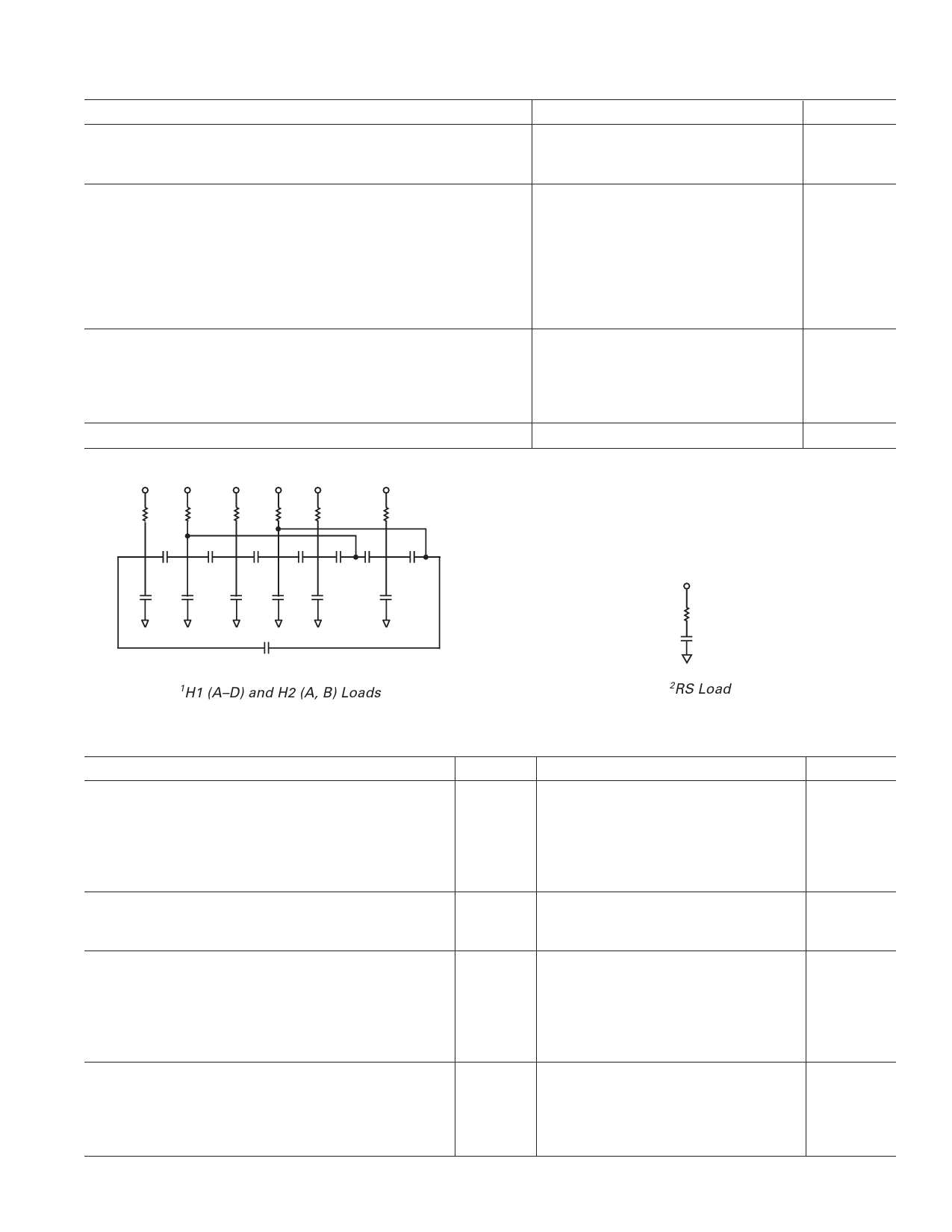
1H1 (A–D) and H2 (A, B) Loads
RS
30⍀
10pF
2RS Load
DIGITAL SPECIFICATIONS (RSVDD = HVDD = 2.7 V to 3.6 V, –25؇C to +85؇C, unless otherwise noted.)
Parameter
Symbol Min
Typ
LOGIC INPUTS (VCKM, SLD, SDA, and SCK)
High Level Input Voltage
VIH
Low Level Input Voltage
VIL
High Level Input Current
IIH
Low Level Input Current
IIL
Input Capacitance
CIN
LOGIC OUTPUTS (Except H1(A–D), H2(A, B), and RS)
High Level Output Voltage @ IOH = 2 mA
VOH
Low Level Output Voltage @ IOL = 2 mA
VOL
H-DRIVER OUTPUTS (H1(A–D), H2(A, B))
High Level Output Voltage @ Max Current
VOH
Low Level Output Voltage @ Max Current
VOL
H1(A–D) Maximum Output Current (Programmable)
H2(A, B) Maximum Output Current (Programmable)
Maximum Load Current
2.1
10
DRVDD – 0.5
DVDD – 0.5
12.25
12.25
100
RS-DRIVER OUTPUTS
High Level Output Voltage @ Max Current
Low Level Output Voltage @ Max Current
RS Maximum Output Current (Programmable)
Maximum Load Current
VOH
RSVDD – 0.5
VOL
12.25
100
Specifications subject to change without notice.
REV. 0
–3–
Max
0.6
40
40
0.5
0.5
0.5
Unit
°C
°C
V
V
V
V
V
V
V
mW
mW
mW
mW
MHz
Unit
V
V
µA
µA
pF
V
V
V
V
mA
mA
pF
V
V
mA
pF
Share Link: 