ADA4817-1ARDZ-R7 查看數據表(PDF) - Analog Devices
零件编号
产品描述 (功能)
生产厂家
ADA4817-1ARDZ-R7 Datasheet PDF : 28 Pages
| |||
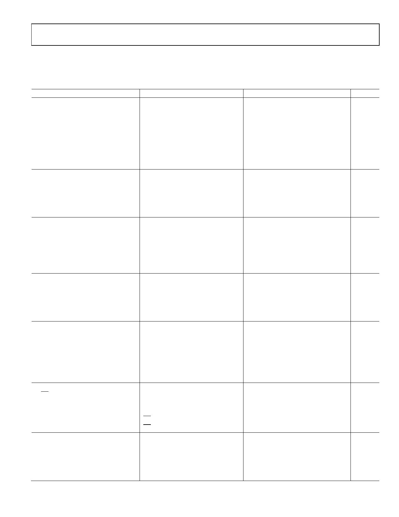
Data Sheet
ADA4817-1/ADA4817-2
SPECIFICATIONS
±5 V OPERATION
TA = 25°C, +VS = 5 V, −VS = −5 V, G = 1, RF = 348 Ω for G > 1, RL = 100 Ω to ground, unless otherwise noted.
Table 1.
Parameter
Conditions
Min
Typ
DYNAMIC PERFORMANCE
−3 dB Bandwidth
Gain Bandwidth Product
Full Power Bandwidth
0.1 dB Flatness
Slew Rate
Settling Time to 0.1%
VOUT = 0.1 V p-p
VOUT = 2 V p-p
VOUT = 0.1 V p-p, G = 2
VOUT = 0.1 V p-p
VIN = 3.3 V p-p, G = 2
VOUT = 2 V p-p, RL = 100 Ω, G = 2
VOUT = 4 V step
VOUT = 2 V step, G = 2
1050
200
390
≥410
60
60
870
9
NOISE/HARMONIC PERFORMANCE
Harmonic Distortion (HD2/HD3)
Input Voltage Noise
f = 1 MHz, VOUT = 2 V p-p, RL = 1 kΩ
f = 10 MHz, VOUT = 2 V p-p, RL = 1 kΩ
f = 50 MHz, VOUT = 2 V p-p, RL = 1 kΩ
f = 100 kHz
−113/−117
−90/−94
−64/−66
4
Input Current Noise
f = 100 kHz
2.5
DC PERFORMANCE
Input Offset Voltage
0.4
Input Offset Voltage Drift
7
Input Bias Current
2
TMIN to TMAX
100
Input Bias Offset Current
1
Open-Loop Gain
62
65
INPUT CHARACTERISTICS
Input Resistance
Common mode
500
Input Capacitance
Common mode
1.3
Differential mode
0.1
Input Common-Mode Voltage Range
Common-Mode Rejection
OUTPUT CHARACTERISTICS
VCM = ±0.5 V
−VS to +VS − 2.8
−77
−90
Output Overdrive Recovery Time
Output Voltage Swing
Linear Output Current
VIN = ±2.5 V, G = 2
RL = 1 kΩ
1% output error
−VS + 1.5 to
+VS − 1.5
−VS + 1.1 to
+VS − 1.1
8
−VS + 1.4 to
+VS − 1.3
−VS + 1 to
+VS − 1
40
Short-Circuit Current
Sinking/sourcing
100/170
POWER-DOWN
PD Pin Voltage
Enabled
>+VS − 1
Turn-On/Turn-Off Time
Powered down
<+VS − 3
0.3/1
Input Leakage Current
PD = +VS
0.3
PD = −VS
34
POWER SUPPLY
Operating Range
5
Quiescent Current per Amplifier
19
Powered Down Quiescent Current
1.5
Positive Power Supply Rejection
+VS = 4.5 V to 5.5 V, −VS = −5 V
−67
−72
Negative Power Supply Rejection
+VS = 5 V, −VS = −4.5 V to −5.5 V
−67
−72
Rev. B | Page 3 of 28
Max Unit
MHz
MHz
MHz
MHz
MHz
MHz
V/µs
ns
dBc
dBc
dBc
nV/√Hz
fA/√Hz
2
mV
µV/°C
20 pA
pA
pA
dB
GΩ
pF
pF
V
dB
ns
V
V
mA
mA
V
V
µs
3
µA
61 µA
10 V
21 mA
3
mA
dB
dB
Share Link: 