ADG3300 查看數據表(PDF) - Analog Devices
零件编号
产品描述 (功能)
生产厂家
ADG3300 Datasheet PDF : 20 Pages
| |||
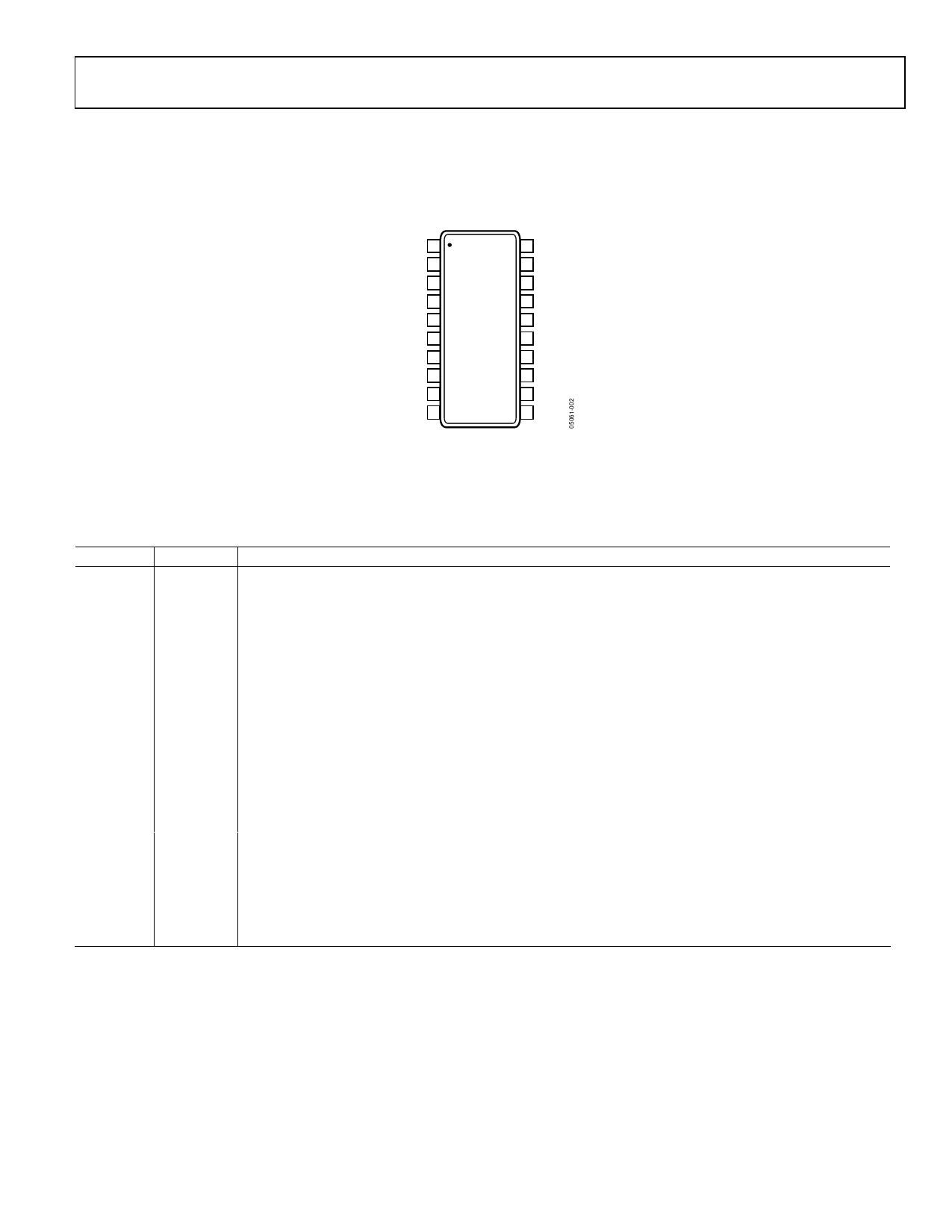
PIN CONFIGURATION AND FUNCTION DESCRIPTIONS
A1 1
20 Y1
VCCA 2
A2 3
A3 4
A4 5
ADG3300
TOP VIEW
(Not to Scale)
19 VCCY
18 Y2
17 Y3
16 Y4
A5 6
15 Y5
A6 7
14 Y6
A7 8
13 Y7
A8 9
12 Y8
EN 10
11 GND
Figure 2. Pin Configuration
Table 3. Pin Function Descriptions
Pin. No. Mnemonic Description
1
A1
Input/Output A1. Referenced to VCCA.
2
VCCA
Power Supply Voltage Input for the A1 to A8 I/O pins (1.15 V ≤ VCCA < VCCY).
3
A2
Input/Output A2. Referenced to VCCA.
4
A3
Input/Output A3. Referenced to VCCA.
5
A4
Input/Output A4. Referenced to VCCA.
6
A5
Input/Output A5. Referenced to VCCA.
7
A6
Input/Output A6. Referenced to VCCA.
8
A7
Input/Output A7. Referenced to VCCA.
9
A8
Input/Output A8. Referenced to VCCA.
10
EN
Active High Enable Input.
11
GND
Ground.
12
Y8
Input/Output Y8. Referenced to VCCY.
13
Y7
Input/Output Y7. Referenced to VCCY.
14
Y6
Input/Output Y6. Referenced to VCCY.
15
Y5
Input/Output Y5. Referenced to VCCY.
16
Y4
Input/Output Y4. Referenced to VCCY.
17
Y3
Input/Output Y3. Referenced to VCCY.
18
Y2
Input/Output Y2. Referenced to VCCY.
19
VCCY
Power Supply Voltage Input for the Y1 to Y8 I/O pins (1.65 V ≤ VCCY ≤ 5.5 V).
20
Y1
Input/Output Y1. Referenced to VCCY.
ADG3300
Rev. 0 | Page 7 of 20
Share Link: 