ADG333A 查看數據表(PDF) - Analog Devices
零件编号
产品描述 (功能)
生产厂家
ADG333A Datasheet PDF : 12 Pages
| |||
ADG333A
SINGLE SUPPLY
VDD = +12 V, VSS = 0 V ± 10%, GND = 0 V, unless otherwise noted.1
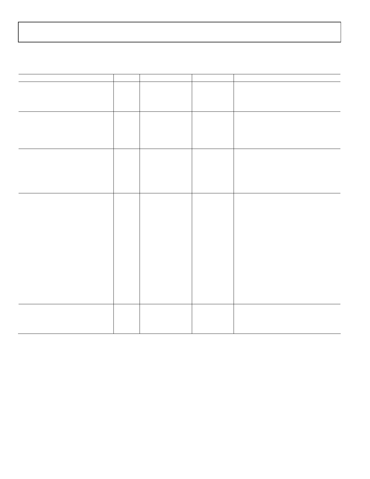
Table 2.
Parameter
ANALOG SWITCH
Analog Signal Range
RON
LEAKAGE CURRENTS
Source OFF Leakage IS (OFF)
Channel ON Leakage ID, IS (ON)
DIGITAL INPUTS
Input High Voltage, VINH
Input Low Voltage, VINL
Input Current
IINL or IINH
DYNAMIC CHARACTERISTICS2
tON
tOFF
Break-Before-Make Delay, tOPEN
+25°C −40°C to +85°C
0 V to VDD
35
75
±0.1
±0.25 ±3
±0.1
±0.4
±5
2.4
0.8
±0.005
±0.5
110
200
100
180
10
Charge Injection
5
OFF Isolation
72
Channel-to-Channel Crosstalk
85
CS (OFF)
CD, CS (ON)
POWER REQUIREMENTS
IDD
VDD
12
25
0.05
0.25
0.35
±3/±30
1 Temperature range is as follows: B Version: −40°C to +85°C.
2 Guaranteed by design; not subject to production test.
Unit
V
Ω typ
Ω max
nA typ
nA max
nA typ
nA max
V min
V max
µA typ
µA max
ns typ
ns max
ns typ
ns max
ns min
ns min
pC typ
dB typ
dB typ
pF typ
pF typ
mA typ
mA max
V min/V max
Test Conditions/Comments
VD = 1 V, 10 V, IS = –1 mA
VDD = 13.2 V
VD = 12.2 V/1 V, VS = 1 V/12.2 V
Figure 15
VS = VD = 12.2 V/1 V
Figure 16
VIN = 0 V or VDD
RL = 300 Ω, CL = 35 pF;
VS = 8 V; Figure 17
RL = 300 Ω, CL = 35 pF;
VS = 8 V; Figure 17
RL = 300 Ω, CL = 35 pF;
VS = 5 V; Figure 18
VD = 6 V, RD = 0 W, CL = 10 nF;
VDD = 12 V, VSS = 0 V; Figure 19
RL = 75 Ω, CL = 5 pF, f = 1 MHz;
VS = 1.15 V rms; Figure 20
RL = 75 Ω, CL = 5 pF, f = 1 MHz;
VS = 1.15 V rms; Figure 21
VDD = 13.5 V
Digital inputs = 0 V or 5 V
Rev. A | Page 4 of 12
Share Link: 