N28F001BX-B90 查看數據表(PDF) - Intel
零件编号
产品描述 (功能)
生产厂家
N28F001BX-B90 Datasheet PDF : 33 Pages
| |||
28F001BX-T 28F001BX-B
290406 – 1
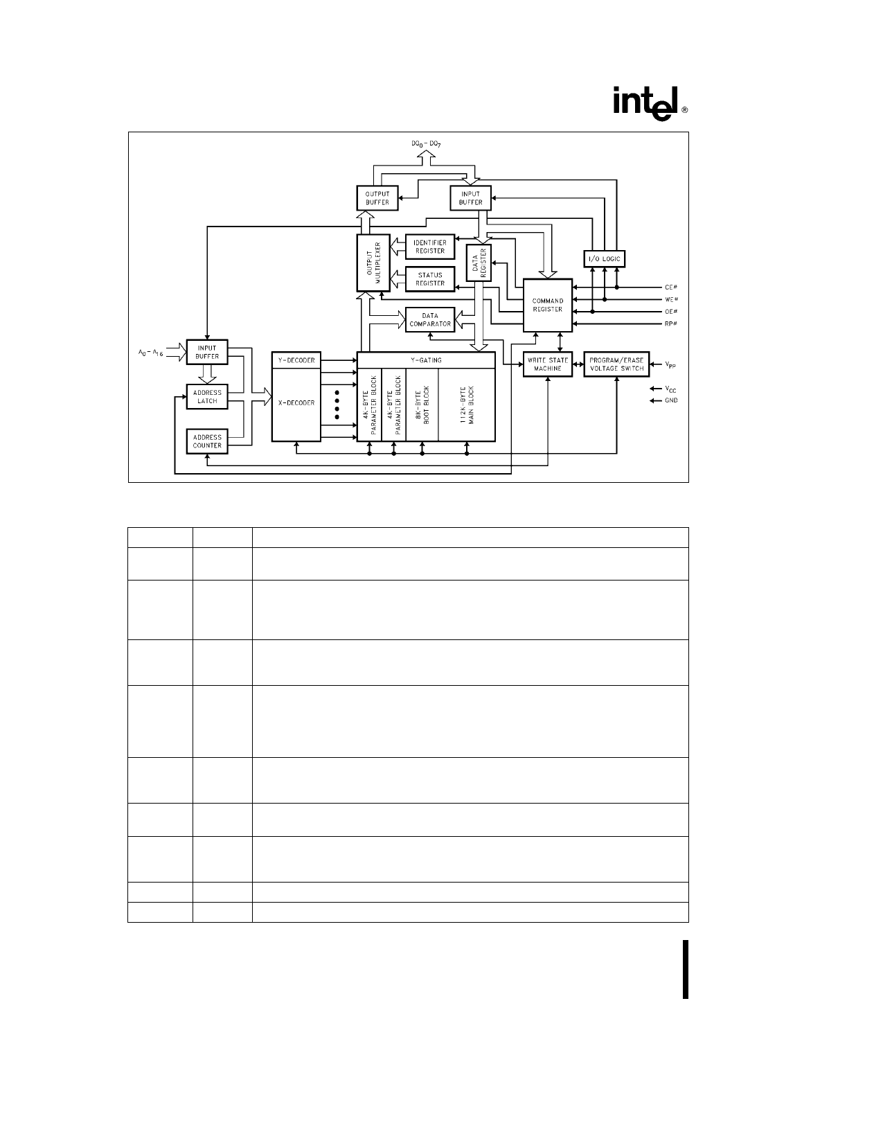
Figure 1 28F001BX Block Diagram
Table 1 Pin Description
Symbol Type
Name and Function
A0 – A16
INPUT ADDRESS INPUTS for memory addresses Addresses are internally latched during
a write cycle
DQ0 – DQ7
INPUT
OUTPUT
DATA INPUTS OUTPUTS Inputs data and commands during memory write
cycles outputs data during memory Status Register and Identifier read cycles The
data pins are active high and float to tri-state off when the chip is deselected or the
outputs are disabled Data is internally latched during a write cycle
CE
INPUT CHIP ENABLE Activates the device’s control logic input buffers decoders and
sense amplifiers CE is active low CE high deselects the memory device and
reduces power consumption to standby levels
RP
INPUT POWERDOWN Puts the device in deep powerdown mode RP is active low
RP high gates normal operation RP e VHH allows programming of the boot
block RP also locks out erase or write operations when active low providing data
protection during power transitions RP active resets internal automation Exit
from deep powerdown sets device to Read Array mode
OE
INPUT OUTPUT ENABLE Gates the device’s outputs through the data buffers during a
read cycle OE is active low OE e VHH (pulsed) allows programming of the
boot block
WE
INPUT WRITE ENABLE Controls writes to the Command Register and array blocks WE
is active low Addresses and data are latched on the rising edge of the WE pulse
VPP
ERASE PROGRAM POWER SUPPLY for erasing blocks of the array or
programming bytes of each block Note With VPP k VPPL max memory contents
cannot be altered
VCC
GND
DEVICE POWER SUPPLY (5V g10%)
GROUND
2
Share Link: 