ADN2807 查看數據表(PDF) - Analog Devices
零件编号
产品描述 (功能)
生产厂家
ADN2807 Datasheet PDF : 21 Pages
| |||
Data Sheet
DEFINITION OF TERMS
MAXIMUM, MINIMUM, AND TYPICAL
SPECIFICATIONS
Specifications for every parameter are derived from statistical
analyses of data taken on multiple devices from multiple wafer
lots. Typical specifications are the mean of the distribution of
the data for that parameter. If a parameter has a maximum (or a
minimum) value, that value is calculated by adding to (or
subtracting from) the mean six times the standard deviation of
the distribution. This procedure is intended to tolerate pro-
duction variations. If the mean shifts by 1.5 standard deviations,
the remaining 4.5 standard deviations still provide a failure rate
of only 3.4 parts per million. For all tested parameters, the test
limits are guardbanded to account for tester variation, and
therefore guarantee that no device is shipped outside of data
sheet specifications.
INPUT SENSITIVITY AND INPUT OVERDRIVE
Sensitivity and overdrive specifications for the quantizer involve
offset voltage, gain, and noise. The relationship between the
logic output of the quantizer and the analog voltage input is
shown in Figure 8. For sufficiently large positive input voltage,
the output is always Logic 1; similarly for negative inputs, the
output is always Logic 0. However, the transitions between
output Logic Levels 1 and 0 are not at precisely defined input
voltage levels, but occur over a range of input voltages. Within
this zone of confusion, the output may be either 1 or 0, or it
may even fail to attain a valid logic state. The width of this zone
is determined by the input voltage noise of the quantizer. The
center of the zone of confusion is the quantizer input offset
voltage. Input overdrive is the magnitude of signal required to
guarantee a correct logic level with a 1 × 10⁻¹⁰ confidence level.
OUTPUT
1
NOISE
0
OFFSET
INPUT (V p-p)
OVERDRIVE
SENSITIVITY
(2× OVERDRIVE)
Figure 8. Input Sensitivity and Input Overdrive
ADN2807
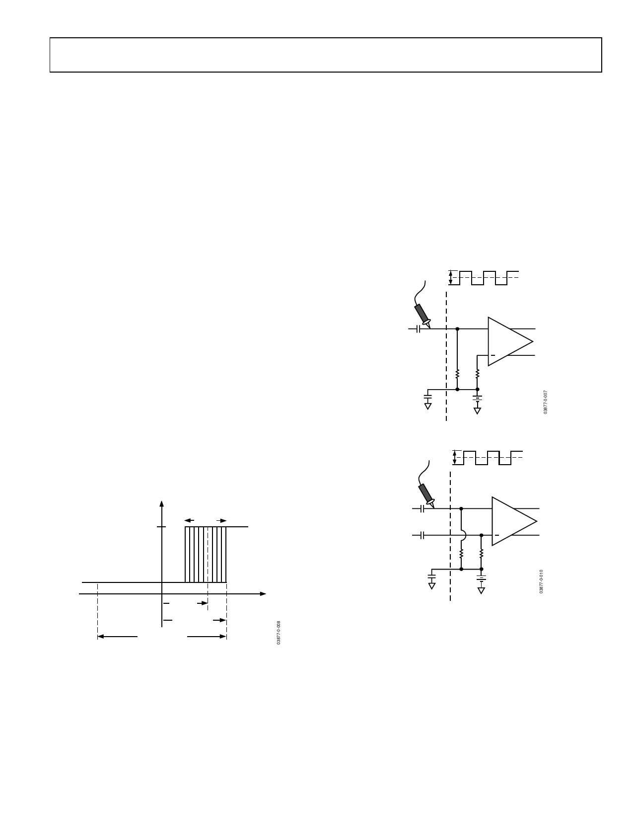
SINGLE-ENDED VS. DIFFERENTIAL
AC coupling typically drives the inputs to the quantizer. The
inputs are internally dc-biased to a common-mode potential of
~0.6 V. Driving the ADN2807 single-ended and observing the
quantizer input with an oscilloscope probe at the point
indicated in Figure 9 shows a binary signal with average value
equal to the common-mode potential and instantaneous values
both above and below the average value. It is convenient to
measure the peak-to-peak amplitude of this signal and call the
minimum required value the quantizer sensitivity. Referring to
Figure 8, since both positive and negative offsets need to be
accommodated, the sensitivity is twice the overdrive.
10mV p-p
VREF
SCOPE
PROBE
ADN2807
PIN
+
QUANTIZER
VREF
50Ω 50Ω
Figure 9. Single-Ended Sensitivity Measurement
5mV p-p
VREF
SCOPE
PROBE
ADN2807
PIN
+
QUANTIZER
NIN
VREF
50Ω 50Ω
Figure 10. Differential Sensitivity Measurement
Driving the ADN2807 differentially (Figure 10), sensitivity
seems to improve by observing the quantizer input with an
oscilloscope probe. This is an illusion caused by the use of a
single-ended probe. A 5 mV p-p signal appears to drive the
ADN2807 quantizer. However, the single-ended probe
measures only half the signal. The true quantizer input signal is
twice this value since the other quantizer input is
complementary to the signal being observed.
Rev. B | Page 9 of 21
Share Link: 