ADN2817ACPZ-RL 查看數據表(PDF) - Analog Devices
零件编号
产品描述 (功能)
生产厂家
ADN2817ACPZ-RL Datasheet PDF : 40 Pages
| |||
Data Sheet
Continuous Rate 10 Mbps to 2.7 Gbps Clock
and Data Recovery ICs
ADN2817/ADN2818
FEATURES
GENERAL DESCRIPTION
Serial data input: 10 Mbps to 2.7 Gbps
Exceeds ITU-T jitter specifications
Integrated limiting amplifier
5 mV p-p sensitivity (ADN2817 only)
Adjustable slice level: ±100 mV (ADN2817 only)
Patented dual-loop clock recovery architecture
Programmable LOS detect (ADN2817 only)
Integrated PRBS generator and detector
No reference clock required
Loss of lock indicator
Supports double data rate
Bit error rate monitor (BERMON) or sample phase adjust options
Rate selectivity without the use of a reference clock
I2C interface to access optional features
Single-supply operation: 3.3 V
Low power
650 mW (ADN2817)
600 mW (ADN2818)
5 mm × 5 mm 32-lead LFCSP
APPLICATIONS
SONET OC-1, OC-3, OC-12, OC-48, and all associated FEC rates
Fibre Channel, 2× Fibre Channel, GbE, HDTV
The ADN2817/ADN2818 provide the receiver functions of
quantization, signal level detect, and clock and data recovery for
continuous data rates from 10 Mbps to 2.7 Gbps. The ADN2817/
ADN2818 automatically lock to all data rates without the need for
an external reference clock or programming. All SONET jitter
requirements are exceeded, including jitter transfer, jitter generation,
and jitter tolerance. All specifications are quoted for −40°C to
+85°C ambient temperature, unless otherwise noted.
This device, together with a PIN diode and a TIA preamplifier,
can implement a highly integrated, low cost, and low power
fiber optic receiver.
The ADN2817/ADN2818 have many optional features available
through an I2C interface. For example, the user can read back
the data rate onto which the ADN2817 or ADN2818 is locked,
or the user can set the device to lock only to one particular data
rate if provisioning of data rates is required. A BERMON circuit
provides an estimate of the received bit error rate (BER) without
interruption of the data. Alternatively, the user can adjust the
data sampling phase to optimize the received BER.
The ADN2817/ADN2818 are available in a compact 5 mm ×
5 mm, 32-lead, lead frame chip scale package.
WDM transponders
Regenerators/repeaters
Test equipment
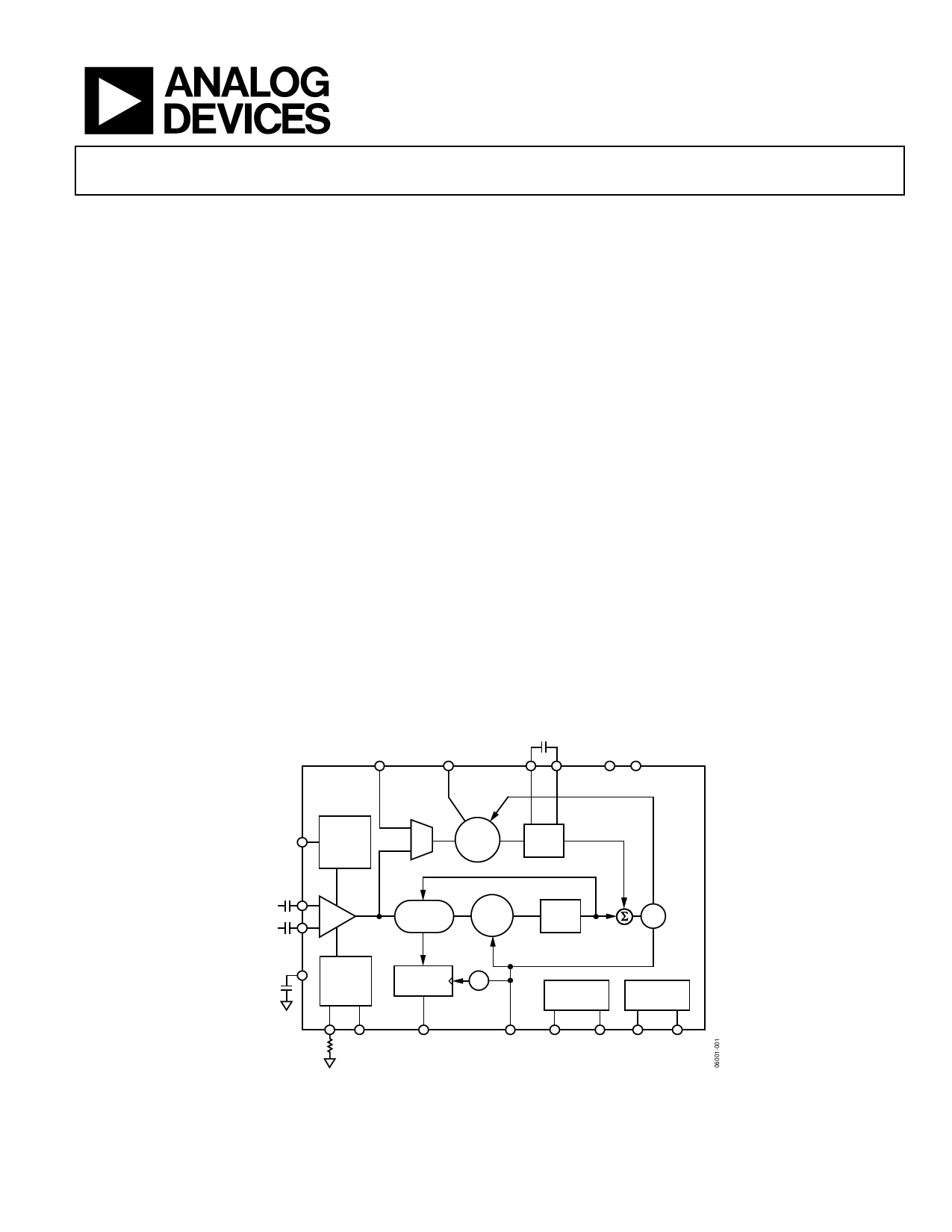
FUNCTIONAL BLOCK DIAGRAM
REFCLKP/REFCLKN
(OPTIONAL)
LOL
CF1
CF2 VCC VEE
ADN2817/ADN2818
SLICEP/
SLICEN
SLICE
ADJUST
(ADN2817
ONLY)
PIN
NIN
VREF
LOS
DETECT
(ADN2817
ONLY)
FREQ/
LOCK
DET
LOOP
FILTER
PHASE
SHIFTER
PHASE
DET
LOOP
FILTER
DATA
RETIMING
ΔФ
BERMON
VCO
I2C
REGISTERS
THRADJ
LOS
DATAOUTP/
DATAOUTN
CLKOUTP/ VBER BERMODE SCK
CLKOUTN
SDA
Figure 1.
Rev. E
Document Feedback
Information furnished by Analog Devices is believed to be accurate and reliable. However, no
responsibility is assumed by Analog Devices for its use, nor for any infringements of patents or other
rights of third parties that may result from its use. Specifications subject to change without notice. No
license is granted by implication or otherwise under any patent or patent rights of Analog Devices.
Trademarks and registered trademarks are the property of their respective owners.
One Technology Way, P.O. Box 9106, Norwood, MA 02062-9106, U.S.A.
Tel: 781.329.4700 ©2007–2013 Analog Devices, Inc. All rights reserved.
Technical Support
www.analog.com
Share Link: 