ADN4612(RevSp0) жҹҘзңӢж•ёж“ҡиЎЁпјҲPDFпјү - Analog Devices
йӣ¶д»¶зј–еҸ·
дә§е“ҒжҸҸиҝ° (еҠҹиғҪ)
з”ҹдә§еҺӮ家
ADN4612 Datasheet PDF : 2 Pages
| |||
Data Sheet
11.3 Gbps 12 Г— 12 Digital Crosspoint
ADN4612
FEATURES
DC to 11.3 Gbps per port NRZ data rate
Multitime constant, programmable receive equalization
Compensates 25 inches of FR408 at 10.3125 Gbps
Compensates 15 inches of FR408 at 11.3 Gbps
6-tap programmable transmit feedforward equalization (FFE)
Compensates 15 inches of FR408 at 10.3125 Gbps
Compensate 10 inches of FR408 at 11.3 Gbps
Low power
150 mW per channel at 2.5 V (outputs enabled)
12 Г— 12, fully differential, nonblocking array
Double rank connection programming
2-pins, selectable connection maps
Per lane loss-of-signal detection
Flexible output termination supply range (1.8 V to 3.3 V)
DC- or ac-coupled differential CML inputs and outputs
Programmable CML output levels
Load from EPROM for automatic power-on ready operation
Per lane input and output P/N pair inversion for routing ease
50 О© on-chip input/output termination
Supports 64-bit/66-bit, scrambled or not coded NRZ data up
to 11.3 Gbps
Serial (I2C or SPI slave) control interface
88-lead LFCSP, 12 mm Г— 12mm, Pb-free package
вҲ’40В°C to +85В°C operating temperature range
APPLICATIONS
Fiber optic network switching
10 Gigabit Ethernet over backplane 10GBASE-KR 802.3ap
XLAUI/CAUI (802.3ba)
SONET OC-192/STM-64x
1Г—, 2Г—, 4Г—, 8Г—, and 10Г— Fibre channel
GENERAL DESCRIPTION
The ADN4612 is a 12 Г— 12 asynchronous, protocol agnostic, digital
crosspoint switch with 12 differential PECL-/CML-compatible
inputs and 12 differential CML outputs.
The ADN4612 is optimized for nonreturn-to-zero (NRZ) signaling
with data rates of up to 11.3 Gbps per port. Each port offers
programmable input equalization, loss-of-signal detection,
programmable output swing, and output preemphasis/deemphasis.
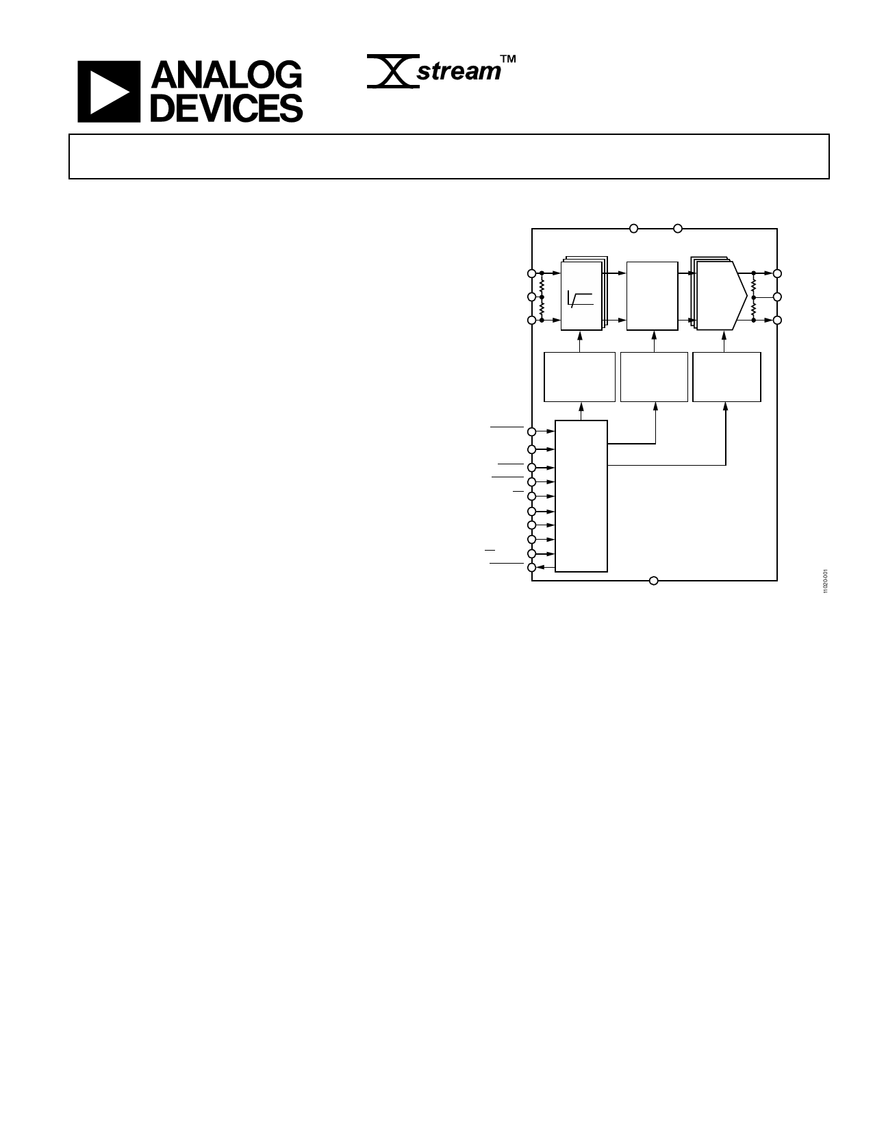
FUNCTIONAL BLOCK DIAGRAM
DVCC
VCC
IP11
TO IP0
RX
TX
OP11
TO OP0
VTTIE,
VTTIW
12 Г— 12
SWITCH
MATRIX
PRE-
EMPHASIS
VTTON,
VTTOS
IN11
EQ
ON11
TO IN0
TO ON0
RX CONTROL
EQUALIZATION
SIGNAL DETECT
XPT CONTROL
CONNECTIVITY
MAP [A/B/C/D]
SELECT
TX CONTROL
6-TAP FFE
OUTPUT LEVEL
EEPROM
MAP1 TO
MAP0
RESET
UPDATE
SPI/I2C
SCK/SCL
SDO/SDA
SDI/I2C_A1
CS/I2C_A0
LOS_IRQ
SERIAL
INTERFACE
CONTROL
LOGIC
ADN4612
VEE
Figure 1.
The ADN4612 nonblocking switch core implements a 12 Г— 12
crossbar and supports independent channel switching through
the serial control interface. The ADN4612 has low latency and
very low channel-to-channel skew.
The ADN4612 is packaged in an 88-lead LFCSP package and
operates from вҲ’40В°C to +85В°C.
For more information about ADN4612, contact Analog Devices, Inc., at xstream@analog.com.
Rev. Sp0
Document Feedback
Information furnished by Analog Devices is believed to be accurate and reliable. However, no
responsibility is assumed by Analog Devices for its use, nor for any infringements of patents or other
rights of third parties that may result from its use. Specifications subject to change without notice. No
license is granted by implication or otherwise under any patent or patent rights of Analog Devices.
Trademarks and registered trademarks are the property of their respective owners.
One Technology Way, P.O. Box 9106, Norwood, MA 02062-9106, U.S.A.
Tel: 781.329.4700
В©2013 Analog Devices, Inc. All rights reserved.
Technical Support
www.analog.com
Share Link: 