ADP3810AR-84 查看數據表(PDF) - Analog Devices
零件编号
产品描述 (功能)
生产厂家
ADP3810AR-84 Datasheet PDF : 16 Pages
| |||
ADP3810/ADP3811
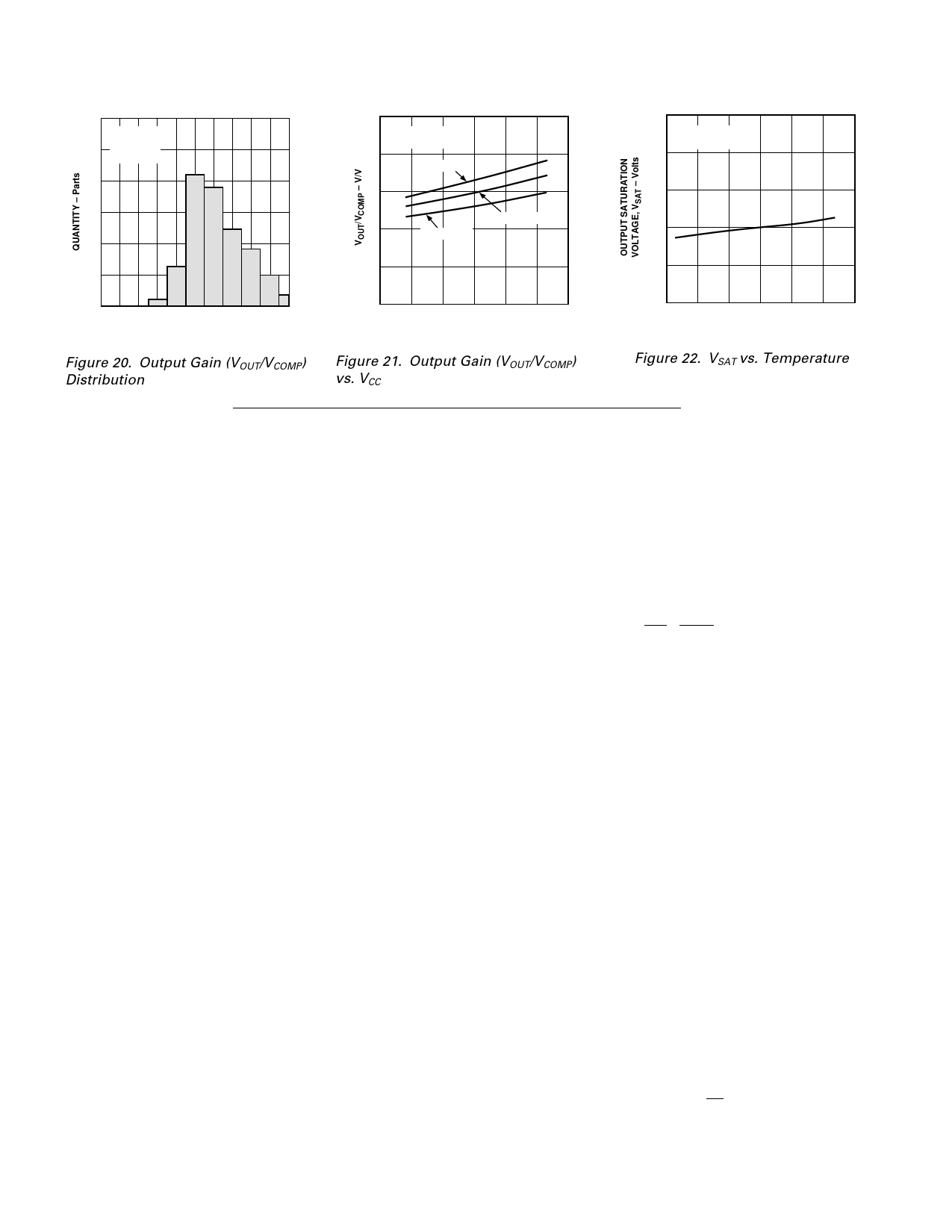
240
VCC = +10V
200
TA = +25°C
RL = 1kΩ
160
120
80
40
0
5.0 5.2 5.4 5.6 5.8 6.0 6.2 6.4 6.6 6.8 7.0
OUTPUT GAIN (VOUT/VCOMP) – V/V
Figure 20. Output Gain (VOUT/VCOMP)
Distribution
8
RL = 1kΩ
VOUT = +1.0V
7
TA = –40°C
6
5
TA = +85°C
TA = +25°C
4
3
0
3
6
9 12 15 18
VCC – Volts
Figure 21. Output Gain (VOUT/VCOMP)
vs. VCC
0.25
0.20
VCC = +10V
ILOAD = 5mA
0.15
0.10
0.05
0
–50 –25 0
25 50 75 100
TEMPERATURE – °C
Figure 22. VSAT vs. Temperature
APPLICATIONS SECTION
Functional Description
The ADP3810 and ADP3811 are designed for charging NiCad,
NiMH and LiIon batteries. Both parts provide accurate voltage
sense and current sense circuitry to control the charge current
and final battery voltage. Figure 1 shows a simplified battery
charging circuit with the ADP3810/ADP3811 controlling an
external dc-dc converter. The converter can be one of many
different types such as a Buck converter, Flyback converter or a
linear regulator. In all cases, the ADP3810/ADP3811 maintains
accurate control of the current and voltage loops, enabling the
use of a low cost, industry standard dc-dc converter without
compromising system performance. Detailed realizations of
complete circuits including the dc-dc converter are included
later in this data sheet.
The ADP3810 and ADP3811 contain the following blocks
(shown in Figure 1):
• Two “GM” type error amplifiers control the current loop
(GM1) and the voltage loop (GM2).
• A common COMP node is shared by both GM amplifiers
such that an RC network at this node helps compensate both
control loops.
• A precision 2.0 V reference is used internally and is available
externally for use by other circuitry. The 0.1 µF bypass ca-
pacitor shown is required for stability.
• A current limited buffer stage (GM3) provides a current out-
put, IOUT, to control an external dc-dc converter. This out-
put can directly drive an optocoupler in isolated converter
applications. The dc-dc converter must have a control scheme
such that higher IOUT results in lower duty cycle. If this is
not the case, a simple, single transistor inverter can be used
for control phase inversion.
• An amplifier buffers the charge current programming volt-
age, VCTRL, to provide a high impedance input.
• An UVLO circuit shuts down the GM amplifiers and the
output when the supply voltage (VCC) falls below 2.7 V. This
protects the charging system from indeterminate operation.
• A transient overshoot comparator quickly increases IOUT
when the voltage on the “+” input of GM2 rises over 120 mV
above VREF. This clamp shuts down the dc-dc converter to
quickly recover from overvoltage transients and protect ex-
ternal circuitry.
Description of Battery Charging Operation
The IC based system shown in Figure 1 charges a battery with a
dc current supplied by a dc-dc converter, which is most likely a
switching type supply but could also be a linear supply where
feasible. The value of the charge current is controlled by the
feedback loop comprised of RCS, R3, GM1, the external dc-dc
converter and a dc voltage at the VCTRL input. The actual
charge current is set by the voltage, VCTRL, and is dependent
upon the choice for the values of RCS and R3 according to the
formula below:
ICHARGE
=1
RCS
×
R3
80 kΩ
×V
CTRL
Typical values are RCS = 0.25 Ω and R3 = 20 kΩ, which result
in a charge current of 1.0 A for a control voltage of 1.0 V. The
80 kΩ resistor is internal to the IC, and it is trimmed to its ab-
solute value. The positive input of GM1 is referenced to
ground, forcing the VCS pin to a virtual ground.
The resistor RCS converts the charge current into the voltage at
VRCS, and it is this voltage that GM1 is regulating. The voltage
at VRCS is equal to –(R3/80 kΩ) VCTRL. When VCTRL equals
1.0 V, VRCS equals –250 mV. If VRCS falls below its pro-
grammed level (i.e., the charge current increases), the negative
input of GM1 goes slightly below ground. This causes the out-
put of GM1 to source more current and drive the COMP node
high, which forces the current, IOUT, to increase. A higher IOUT
decreases the drive to the dc-dc converter, reducing the charg-
ing current and balancing the feedback loop.
As the battery approaches its final charge voltage, the voltage
loop takes over. The system becomes a voltage source, floating
the battery at constant voltage thereby preventing overcharging.
The constant voltage feature also protects the circuitry that is
actually powered by the battery from overvoltage if the battery is
removed. The voltage loop is comprised of R1, R2, GM2 and
the dc-dc converter. The final battery voltage is simply set by
the ratio of R1 and R2 according to the following equation
(VREF = 2.000 V):
V BAT
= 2.000V
×
R1
R2
+
1
If the battery voltage rises above its programmed voltage,
VSENSE is pulled above VREF. This causes GM2 to source more
current, raising the COMP node voltage and IOUT. As with the
–6–
REV. 0
Share Link: 