ADP5023(RevA) 查看數據表(PDF) - Analog Devices
零件编号
产品描述 (功能)
生产厂家
ADP5023 Datasheet PDF : 28 Pages
| |||
Data Sheet
ADP5023
LDO SPECIFICATIONS
VIN3 = (VOUT3 + 0.5 V) or 1.7 V (whichever is greater) to 5.5 V; CIN = COUT = 1 µF; TJ = −40°C to +125°C for minimum/maximum
specifications, and TA = 25°C for typical specifications, unless otherwise noted.1
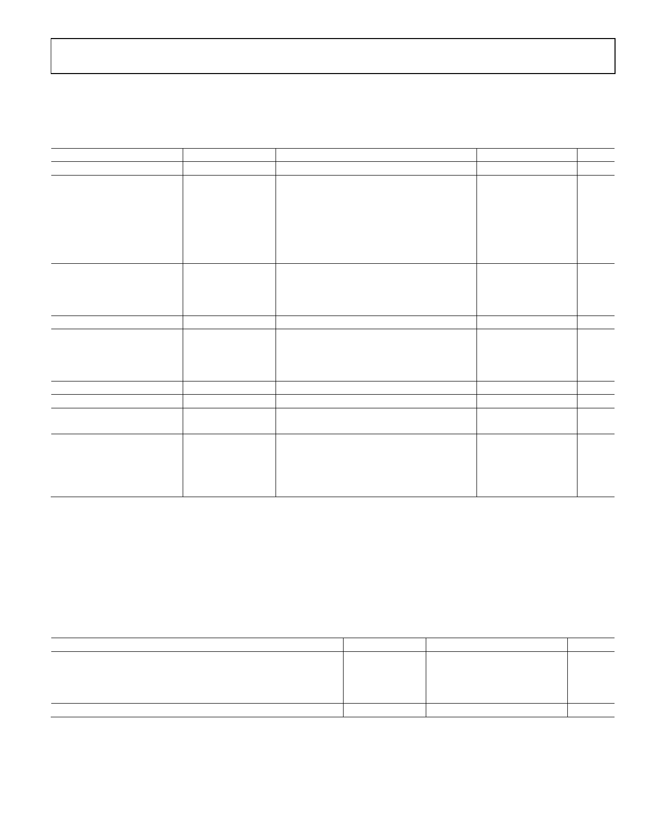
Table 3.
Parameter
INPUT VOLTAGE RANGE
OPERATING SUPPLY CURRENT
Bias Current per LDO2
Total System Input Current
LDO Only
OUTPUT CHARACTERISTICS
Output Voltage Accuracy
Line Regulation
Load Regulation3
VOLTAGE FEEDBACK
DROPOUT VOLTAGE4
CURRENT-LIMIT THRESHOLD5
ACTIVE PULL-DOWN
OUTPUT NOISE
Regulator LDO
POWER SUPPLY REJECTION
RATIO
Regulator LDO
Symbol
VIN3
IVIN3BIAS
IIN
ΔVOUT3/VOUT3
(ΔVOUT3/VOUT3)/ΔVIN3
(ΔVOUT3/VOUT3)/ΔIOUT3
VFB3
VDROPOUT
ILIMIT3
RPDWN-L
NOISELDO
PSRR
Test Conditions/Comments
IOUT3 = 0 µA
IOUT3 = 10 mA
IOUT3 = 300 mA
Includes all current into AVIN, VIN1, VIN2, and
VIN3
IOUT3 = 0 µA, all other channels disabled
100 µA < IOUT3 < 300 mA
IOUT3 = 1 mA
IOUT3 = 1 mA to 300 mA
VOUT3 = 5.2 V, IOUT3 = 300 mA
VOUT3 = 3.3 V, IOUT3 = 300 mA
VOUT3 = 2.5 V, IOUT3 = 300 mA
VOUT3 = 1.8 V, IOUT3 = 300 mA
Channel disabled
10 Hz to 100 kHz, VIN3 = 5 V, VOUT3 = 2.8 V
10 kHz, VIN3 = 3.3 V, VOUT3 = 2.8 V, IOUT3 = 1 mA
100 kHz, VIN3 = 3.3 V, VOUT3 = 2.8 V, IOUT3 = 1 mA
1 MHz, VIN3 = 3.3 V, VOUT3 = 2.8 V, IOUT3 = 1 mA
Min Typ Max Unit
1.7
5.5 V
10 30 µA
60 100 µA
165 245 µA
53
µA
−3
−0.03
0.485
335
0.001
0.5
50
75
100
180
600
600
+3
+0.03
0.003
0.515
140
%
%/V
%/mA
V
mV
mV
mV
mV
mA
Ω
100
µV rms
60
dB
62
dB
63
dB
1 All limits at temperature extremes are guaranteed via correlation using standard statistical quality control (SQC).
2 This is the input current into VIN3, which is not delivered to the output load.
3 Based on an endpoint calculation using 1 mA and 300 mA loads.
4 Dropout voltage is defined as the input-to-output voltage differential when the input voltage is set to the nominal output voltage. This applies only to output voltages
above 1.7 V.
5 Current-limit threshold is defined as the current at which the output voltage drops to 90% of the specified typical value. For example, the current limit for a 3.0 V
output voltage is defined as the current that causes the output voltage to drop to 90% of 3.0 V, or 2.7 V.
INPUT AND OUTPUT CAPACITOR, RECOMMENDED SPECIFICATIONS
TA = −40°C to +125°C, unless otherwise specified.
Table 4.
Parameter
NOMINAL INPUT AND OUTPUT CAPACITOR RATINGS
BUCK1, BUCK2 Input Capacitor Ratings
BUCK1, BUCK2 Output Capacitor Ratings
LDO1 Input and Output Capacitor Ratings
CAPACITOR ESR
Symbol
CMIN1, CMIN2
CMIN1, CMIN2
CMIN3, CMIN4
RESR
Min
4.7
10
1.0
0.001
Typ
Max
Unit
40
µF
40
µF
µF
1
Ω
1 The minimum input and output capacitance should be greater than 0.70 µF over the full range of operating conditions. The full range of operating conditions in
the application must be considered during device selection to ensure that the minimum capacitance specification is met. X7R- and X5R-type capacitors are
recommended; Y5V and Z5U capacitors are not recommended for use because of their poor temperature and dc bias characteristics.
Rev. A | Page 5 of 28
Share Link: 