GS8180D18D-250I 查看數據表(PDF) - Giga Semiconductor
零件编号
产品描述 (功能)
生产厂家
GS8180D18D-250I Datasheet PDF : 28 Pages
| |||
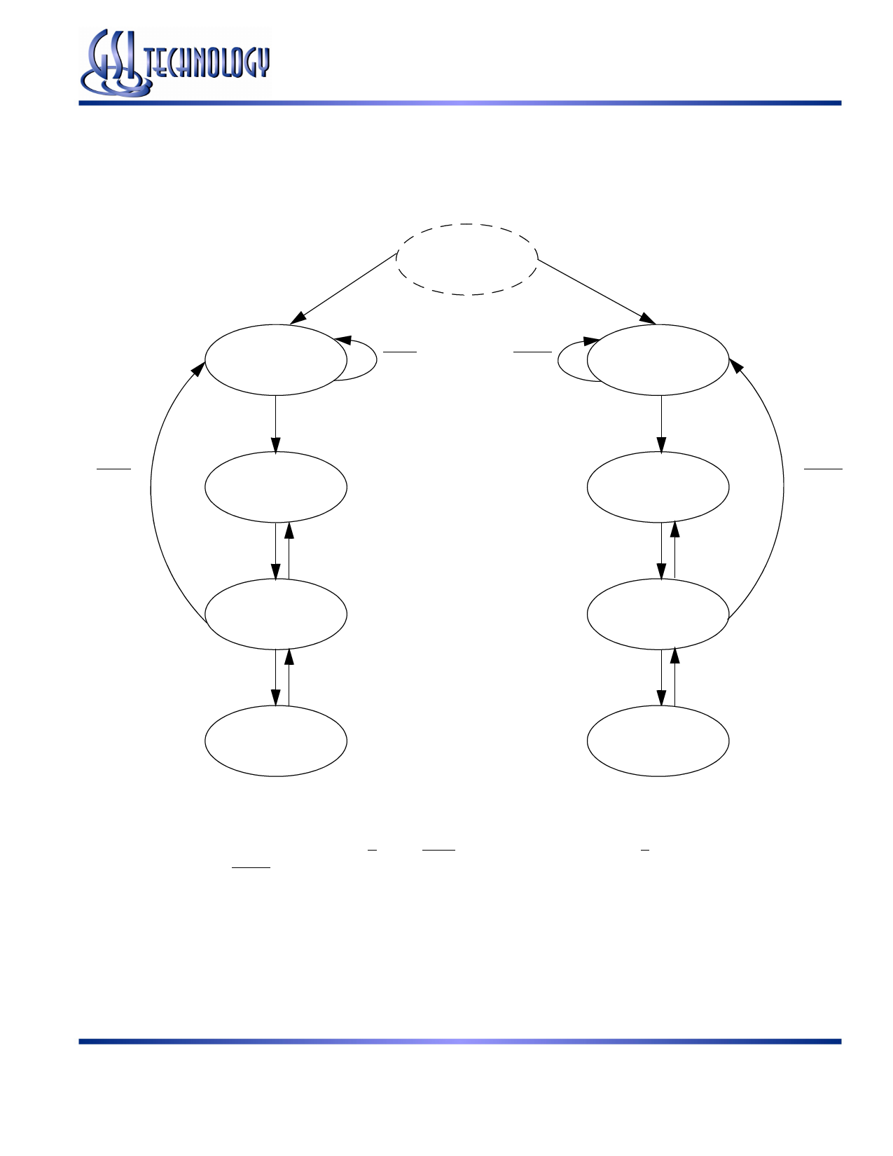
State Diagram
GS8180D18D-250/200/167/133/100
Power-
READ
R Count = 2
Read NOP
READ
READ
Load New
Read Address
R Count = 0
Always
READ
R Count = 2
DDR Read
R Count = R Count + 1
READ
R Count = 1
Always
Increment
Read Address
WRITE
Write NOP
WRITE
Load New
Write Address
W Count = 0
Always
WRITE
W Count = 2
WRITE
W Count = 2
DDR Write
W Count = W Count + 1
Always
WRITE
W Count = 1
Increment
Write Address
Notes:
1. Internal burst counter is fixed as 2-bit linear (i.e., when first address is A0+), next internal burst address is A0+1.
2. “READ” refers to read active status with R = Low, “READ” refers to read inactive status with R = High. The same is true for
“WRITE” and “WRITE”.
3. Read and write state machine can be active simultaneously.
4. State machine control timing sequence is controlled by K.
5. R Count is the read counter; Burst of 4 must complete 2 DDR reads.
6. W Count is the write counter; Burst of 4 must complete 2 DDR writes.
Rev: 2.04 4/2005
11/28
Specifications cited are subject to change without notice. For latest documentation see http://www.gsitechnology.com.
© 2002, GSI Technology
Share Link: 