ADSP-21MOD870 查看數據表(PDF) - Analog Devices
零件编号
产品描述 (功能)
生产厂家
ADSP-21MOD870 Datasheet PDF : 32 Pages
| |||
ADSP-21mod870
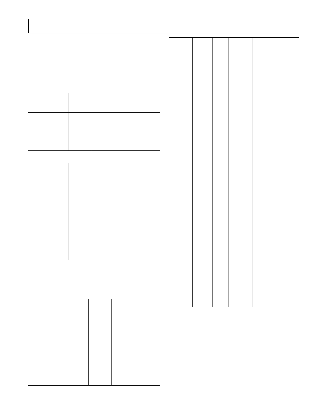
Memory Interface Pins
The ADSP-21mod870 processor can be used in one of two
modes: Full Memory Mode, which allows BDMA operation
with full external overlay memory and I/O capability, or Host
Mode, which allows IDMA operation with limited external
addressing capabilities. The operating mode is determined by
the state of the Mode C pin during RESET and cannot be
changed while the processor is running.
Full Memory Mode Pins (Mode C = 0)
Pin Name
A13:0
D23:0
#
of
Pins
14
24
Input/
Output
O
I/O
Function
Address Output Pins for Pro-
gram, Data, Byte and I/O Spaces
Data I/O Pins for Program,
Data, Byte and I/O Spaces
(8 MSBs Are Also Used as
Byte Memory Addresses)
Host Mode Pins (Mode C = 1)
#
of Input/
Pin Name Pins Output Function
IAD15:0 16 I/O
A0
1
O
D23:8
IWR
IRD
IAL
IS
IACK
16 I/O
1
I
1
I
1
I
1
I
1
O
IDMA Port Address/Data Bus
Address Pin for External I/O,
Program, Data, or Byte Access
Data I/O Pins for Program,
Data Byte and I/O Spaces
IDMA Write Enable
IDMA Read Enable
IDMA Address Latch Pin
IDMA Select
IDMA Port Acknowledge
Configurable in Mode D; Open
Drain
In Host Mode, external peripheral addresses can be decoded using the A0,
CMS, PMS, DMS and IOMS signals.
Terminating Unused Pin
The following table shows the recommendations for terminating
unused pins.
Pin Terminations
Pin
Name
I/O
3-State
(Z)
Reset
State
Hi-Z*
Caused
By
Unused
Configuration
XTAL
CLKOUT
A13:1 or
IAD12:0
A0
D23:8
D7 or
IWR
D6 or
IRD
D5 or
IAL
I
O
O (Z)
I/O (Z)
O (Z)
I/O (Z)
I/O (Z)
I
I/O (Z)
I
I/O (Z)
I
I
O
Hi-Z
Hi-Z
Hi-Z
Hi-Z
Hi-Z
I
Hi-Z
I
Hi-Z
I
BR, EBR
IS
BR, EBR
BR, EBR
BR, EBR
BR, EBR
BR, EBR
BR, EBR
Float
Float
Float
Float
Float
Float
Float
High (Inactive)
Float
High (Inactive)
Float
Low (Inactive)
D4 or
IS
D3 or
IACK
D2:0 or
IAD15:13
PMS
DMS
BMS
IOMS
CMS
RD
WR
BR
BG
BGH
IRQ2/PF7
I/O (Z)
I
I/O (Z)
**
I/O (Z)
I/O (Z)
O (Z)
O (Z)
O (Z)
O (Z)
O (Z)
O (Z)
O (Z)
I
O (Z)
O (Z)
I/O (Z)
Hi-Z
I
Hi-Z
**
Hi-Z
Hi-Z
O
O
O
O
O
O
O
I
O
O
I
IRQL1/PF6 I/O (Z) I
IRQL0/PF5 I/O (Z) I
IRQE/PF4 I/O (Z) I
SCLK0
I/O
I
RFS0
I/O
I
DR0
I
I
TFS0
I/O
O
DT0
O
O
SCLK1
I/O
I
RFS1/IRQ0 I/O
I
DR1/FI
I
I
TFS1/IRQ1 I/O
O
DT1/FO O
O
EE
I
I
EBR
I
I
EBG
O
O
ERESET I
I
EMS
O
O
EINT
I
I
ECLK
I
I
ELIN
I
I
ELOUT O
O
BR, EBR
BR, EBR
BR, EBR
IS
BR, EBR
BR, EBR
BR, EBR
BR, EBR
BR, EBR
BR, EBR
BR, EBR
EE
EE
Float
High (Inactive)
Float
Float
Float
Float
Float
Float
Float
Float
Float
Float
Float
High (Inactive)
Float
Float
Input = High (Inactive)
or Program as Output,
Set to 1, Let Float
Input = High (Inactive)
or Program as Output,
Set to 1, Let Float
Input = High (Inactive)
or Program as Output,
Set to 1, Let Float
Input = High (Inactive)
or Program as Output,
Set to 1, Let Float
Input = High or Low,
Output = Float
High or Low
High or Low
High or Low
Float
Input = High or Low,
Output = Float
High or Low
High or Low
High or Low
Float
NOTES
**Hi-Z = High Impedance.
**Determined by MODE D pin:
Mode D = 0 and in host mode: IACK is an active, driven signal and cannot
be “wire ORed.”
Mode D = 1 and in host mode: IACK is an open source and requires an
external pull-down, but multiple IACK pins can be “wire ORed” together.
1. If the CLKOUT pin is not used, turn it OFF.
2. If the Interrupt/Programmable Flag pins are not used, there are two options:
Option 1: When these pins are configured as INPUTS at reset and function
as interrupts and input flag pins, pull the pins High (inactive).
Option 2: Program the unused pins as OUTPUTS, set them to 1, and let
them float.
3. All bidirectional pins have three-stated outputs. When the pins is configured
as an output, the output is Hi-Z (high impedance).
4. CLKIN, RESET, and PF3:0 are not included in the table because these pins
must be used.
REV. 0
–5–
Share Link: 